The Missing Motherboard for Quantum Computers May Be Superconducting
Quantum computers are usually introduced with one number: how many qubits they have.
That number matters. But every new qubit also creates a much less glamorous engineering problem.
It needs control signals. It needs readout. It needs cables running between room-temperature electronics and a processor sitting deep inside a cryostat. Those cables have to pass through several temperature stages without adding more heat, congestion or hardware than the refrigerator can comfortably support.
So scaling a quantum computer is not only a question of building more qubits.
The classical control system has to scale with them.
A newly launched Finnish company called S-Transistors is building around that second problem. The VTT spinout announced on August 31, 2026 that it has raised €2.6 million to develop integrated circuits based on superconducting transistors, with a first product planned as a cryogenic multiplexer and a longer-term goal the company calls a “quantum motherboard.”
The funding is the news.
The control architecture is the interesting part.
More Qubits Create a Classical Electronics Problem
A superconducting quantum processor operates at temperatures measured in millikelvin.
Much of the equipment that tells it what to do does not.
Today, signal generation, control and part of the readout stack can sit at room temperature, connected to the quantum processor through coaxial cables and other wiring that descend through the dilution refrigerator.
This works. It is also one reason engineers keep studying ways to move more classical electronics into the cold environment.
The scaling relationship is easy to see.
If every additional group of qubits requires additional dedicated control and readout connections, the processor does not grow alone. The wiring, connectors, filters, amplifiers, control hardware and thermal load grow around it.
This is not just S-Transistors’ framing.
A 2026 Nature Electronics paper on superconducting digital control described individual signal lines as a major scaling challenge and demonstrated digital demultiplexing at millikelvin temperatures to distribute control pulses across multiple qubits.
The qubit count and the control stack are two sides of the same machine.
The Cryostat Has a Thermal Budget
Moving electronics closer to the quantum processor sounds straightforward until temperature enters the design.
At the coldest stages of a dilution refrigerator, cooling power is extremely limited.
That means an electronic circuit sitting near the qubits has to do useful work without turning its electrical power into more heat than the refrigerator can remove.
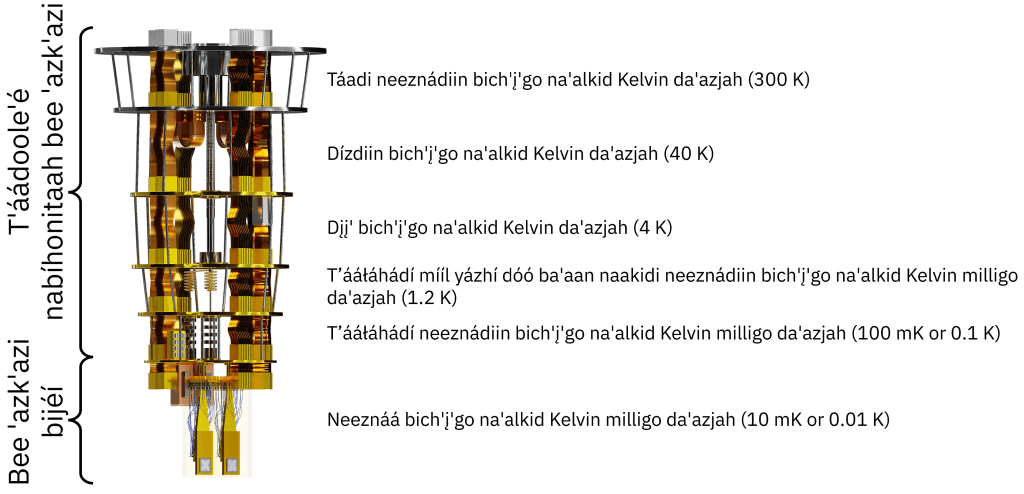
This is why cryogenic control research is not simply about shrinking room-temperature electronics and putting them inside the cryostat.
Power dissipation, thermal noise, cross-coupling and signal integrity all matter.
Researchers have already demonstrated several routes, including cryogenic CMOS and superconducting digital logic. A 2023 Nature Electronics study, for example, demonstrated a low-power cryo-CMOS multiplexer below 15 millikelvin while maintaining high single-qubit gate fidelity with appropriate filtering.
S-Transistors is entering the same broader problem from a different device layer.
Instead of beginning with conventional transistor logic adapted to cryogenic operation, it is trying to build control circuits around a transistor whose switching behavior is tied directly to superconductivity.
What S-Transistors Is Actually Building
The company’s core device is a superconducting transistor.
More specifically, the underlying VTT research describes a Josephson field-effect transistor, or JoFET.
A JoFET combines a gate-controlled transistor-like structure with a superconducting weak link. Instead of using the gate only to control an ordinary semiconductor channel, the gate can tune the superconducting current flowing through the device.
That gives engineers something unusually useful for cryogenic electronics: electrical control in a device designed to operate in the same low-temperature world as superconducting circuits.
The S-Transistors announcement describes the goal as combining transistor functionality with the ultra-low power dissipation associated with superconductivity.
That is an important distinction.
The company is not claiming that every circuit consumes literally zero power. The engineering target is to make control and signal-routing electronics far more compatible with the thermal constraints of a cryogenic quantum system.
The transistor is the building block.
The real question is what can be built around enough of them.
The Device Starts With Graphene and a Josephson Junction
The technical foundation is more concrete than the startup announcement alone suggests.
A 2024 Applied Physics Letters paper from VTT and Aalto University reported wafer-scale, CMOS-compatible graphene Josephson field-effect transistors.
The devices used monolayer graphene as the channel, an aluminum-oxide gate dielectric, and superconducting titanium/aluminum contacts.
The researchers demonstrated gate-tunable superconducting critical current across devices with gate lengths between 150 and 350 nanometers. For one 50-micrometer-wide device, the paper reports critical current reaching roughly 3 microamps.
The exact values are less important than what they establish.
The transistor can be controlled electrically.
The superconducting behavior is measurable and repeatable.
And the fabrication process was designed around wafer-scale methods rather than a single hand-built laboratory device.
That is the bridge between a physics experiment and something that might eventually become an integrated circuit platform.
Wafer-Scale Is the Part That Changes the Conversation
A superconducting transistor is interesting as a device.
A reproducible wafer process is what makes circuits possible.
VTT’s current announcement says the technology is already available at wafer scale. Earlier research provides useful detail behind that statement.
A 2025 VTT/Aalto conference paper on graphene JoFET fabrication reported a 98% device yield on a 150 mm wafer platform. The researchers also developed behavioral and physics models intended to support circuit design.
That does not mean a complete quantum motherboard is rolling off a production line today.
It means the work has moved beyond proving that one transistor can switch.
Integrated electronics require repeatability across many devices, predictable models for circuit designers, process control and eventually a manufacturing path that can produce useful circuits at acceptable yield.
S-Transistors is now trying to take that next step.
The company says part of its new funding will go toward establishing a manufacturing pilot line for superconducting-transistor integrated circuits.
The First Product Is a Multiplexer, Not a Motherboard
The words “quantum motherboard” make the long-term vision easy to imagine.
The first product is much narrower.
S-Transistors says it plans to build a superconducting-transistor-based multiplexer that plugs into existing cryogenic setups.
That sequencing makes engineering sense.
A multiplexer takes multiple signal paths and allows them to share a smaller number of physical connections or routing resources. Inside a cryogenic system, that can reduce some of the wiring burden without asking a quantum-computer developer to redesign the entire control architecture at once.
The company says the first multiplexer is intended for quantum-device development and prototyping and is planned to reach early customers and strategic partners within its first year of operation.
That creates a clean progression:
one transistor,
then a useful routing circuit,
then denser integrated control electronics,
and eventually the larger motherboard concept.
The motherboard is the destination.
The multiplexer is the first test of whether the device platform can become a product.
Why Multiplexing Matters So Much at Millikelvin Temperatures
Multiplexing is not a new idea in quantum hardware.
It keeps appearing because it attacks one of the most physical parts of the scaling problem: the number of wires entering a cryostat.
A 2025 Nature Communications paper on superconducting time-division multiplexing describes each signal line as a contributor to cryostat cost, occupied space and temperature stability.
A separate 2026 Nature Electronics demonstration integrated superconducting digital control electronics with qubits at millikelvin temperature and used digital demultiplexing to distribute control pulses across several qubits.
The approaches are different, but the design goal is related.
Instead of allowing the number of room-temperature connections to rise directly with every new controlled element, place smarter routing closer to the quantum device.
S-Transistors wants its first product to occupy exactly that layer.
If the multiplexer works as intended in existing cryogenic setups, the company gets to test the transistor technology in the place where its claimed advantage matters most: inside a real cold signal path.
A Quantum Motherboard Is Not a PC Motherboard
The analogy is useful, but it needs limits.
A PC motherboard connects a processor, memory, storage, expansion devices, power delivery and external interfaces on a shared physical platform.
S-Transistors is not proposing that same architecture at millikelvin temperature.
Its “quantum motherboard” refers to an integrated cryogenic control layer that sits much closer to the quantum processing unit and handles more of the signal orchestration locally.
Think of it as the missing classical layer around the QPU.
The quantum chip still performs quantum operations.
Room-temperature computers still participate in the wider system.
But some of the work that currently requires large numbers of individual connections between those worlds could move into cryogenic integrated circuits.
That is why the motherboard idea matters.
It shifts the scaling question from:
How many qubits can we fabricate?
to:
How many qubits can the complete machine control, read and connect without the surrounding infrastructure becoming the limiting factor?
The Control Layer May Need to Move Closer to the QPU
The closer control electronics move to the quantum processor, the less distance some signals need to travel before they are routed, selected or processed.
That can reduce wiring pressure.
It also changes the engineering tradeoffs.
Electronics closer to the qubits must coexist with a far more delicate thermal and electromagnetic environment than ordinary control hardware.
Cryogenic CMOS research has shown that transistor-based electronics can operate at very low temperatures. Superconducting digital logic has shown another route. Recent work has even demonstrated integrated quantum processors controlled by superconducting digital electronics at millikelvin temperature.
S-Transistors does not need those approaches to be wrong for its own approach to matter.
They establish something broader: quantum scaling increasingly includes co-design between the QPU and its classical control electronics.
The company is betting that a gate-controlled superconducting transistor can become a useful building block inside that co-design.
That is a more precise claim than saying one device will solve quantum scaling by itself.
The Motherboard Has to Be an Integrated Circuit Problem
One transistor can route one thing.
A motherboard requires systems of devices.
That is why S-Transistors’ move from wafer-scale JoFETs toward integrated circuits is the critical transition.
Circuit designers need device models.
Fabrication needs repeatability.
Logic and routing need predictable switching.
The architecture needs interfaces to the quantum hardware it is supposed to control.
Packaging has to survive repeated cryogenic cycles.
And the complete circuit has to fit inside a thermal budget that gets tighter as it moves closer to the coldest stage.
The earlier VTT research already addresses part of that foundation by reporting wafer-scale fabrication and developing models for JoFET-based circuits.
The new company is taking on the next layer: product prototypes, a dedicated cryogenic laboratory and a pilot manufacturing line.
That is why the €2.6 million round matters without becoming the center of the story.
It funds the transition from device physics into circuit engineering.
There Is More Than One Route to Cryogenic Control
Quantum hardware is not waiting for a single control technology.
Cryo-CMOS, superconducting single-flux-quantum circuits, adiabatic superconducting logic and other cryogenic electronics are all active areas of research.
That context is useful because it keeps the S-Transistors story in proportion.
A 2024 npj Quantum Information paper on adiabatic superconductor logic described the very small cooling power available near 10 millikelvin as a central constraint for conventional logic families close to qubits.
A 2026 Nature Electronics system showed that superconducting digital electronics can already control multiple qubits at millikelvin temperature with digital demultiplexing.
S-Transistors adds another device architecture to that landscape.
Its differentiator is the attempt to retain familiar field-effect transistor control while using a superconducting channel structure designed for extremely low-temperature operation.
The winner does not need to be one universal technology.
Future quantum computers may partition different control tasks across different temperature stages and different electronic technologies.
What Has Been Demonstrated, and What Is Still Planned
This is where the timeline needs to stay clear.
Already demonstrated in the underlying research:
wafer-scale graphene JoFET fabrication,
CMOS-compatible processing,
gate-tunable superconducting critical current,
and later work reporting high device yield on a 150 mm wafer platform.
Announced by S-Transistors:
a €2.6 million pre-seed round,
development of cryogenic signal-control prototypes,
a dedicated cryogenic laboratory,
a manufacturing pilot line,
and a superconducting-transistor multiplexer planned as the first product.
Still a longer-term goal:
the complete quantum motherboard.
That separation matters because a transistor platform and a finished control architecture are not the same thing.
The technical foundation exists.
The company now has to turn that foundation into circuits that quantum-hardware teams can integrate, characterize and use.
That is the stage the story is at today.
Why the 150 mm Wafer Matters More Than the Funding Number
Deep-tech announcements often lead with the size of the investment.
For this story, the more interesting number may be 150 millimeters.
That is the wafer size used in the 2025 fabrication work that reported 98% yield for the graphene JoFET platform.
A wafer result says something different from a funding round.
It says the researchers are thinking about process repeatability across many devices at once.
It also exposes the next questions naturally.
Can those devices be connected into larger circuits with consistent behavior?
Can useful multiplexers be fabricated with the same repeatability?
How does performance change when the circuit is packaged and connected to real quantum hardware?
What power, noise and switching characteristics appear at system level?
S-Transistors has not answered all of those questions publicly yet.
Its product roadmap is designed to start answering them.
That is a healthy way to read the announcement: not as the completion of a quantum motherboard, but as the beginning of the circuit-validation phase.
The Next Scaling Metric May Be Connections per Qubit
Qubit counts are easy to put on a chart.
Control architecture is harder to compress into one number.
But as systems grow, the ratio between quantum devices and the classical hardware needed to operate them may become just as important.
How many external lines are required?
How much control can be multiplexed?
How much power is dissipated at each temperature stage?
How much signal processing or routing can move closer to the QPU?
How much hardware sits outside the cryostat for every useful operation inside it?
Those questions do not replace qubit quality, gate fidelity or error correction.
They sit beside them.
A scalable quantum computer has to scale as a whole machine.
That is the deeper reason a superconducting multiplexer is worth watching even though it sounds much less dramatic than a new quantum processor.
Sometimes the limiting component is not the thing doing the computation.
It is the infrastructure that lets the computation happen.
The Real Upgrade Is Moving From More Qubits to a Scalable Machine
S-Transistors has attached a memorable name to its long-term goal: the quantum motherboard.
The name works because it points at a layer that is easy to ignore.
A quantum processor cannot scale independently from the classical system that controls it.
More qubits eventually mean more routing, more readout, more interfaces and more decisions about where electronics should live inside the temperature stack.
Superconducting transistors offer one possible way to move part of that work into the cryogenic environment without asking conventional room-temperature electronics to follow every signal all the way down.
The technology is not at the motherboard stage yet.
The first product is a multiplexer.
Before that sits a wafer-scale JoFET process.
Before that sits the physics of a gate-controlled superconducting current.
That chain is what makes the story interesting.
The next major upgrade in quantum computing may not arrive as another qubit.
It may arrive as the hardware that finally lets thousands of them behave like one scalable machine.
CXL 4.0 Pushes Memory Further Toward a Shared System Resource
Server memory has traditionally been planned around one host. A processor owns a set of memory channels. DIMMs are installed for that server. Capacity is sized around the workloads expected to run there.
CXL changes that model by allowing memory to sit behind a coherent interconnect instead of existing only on the processor’s local memory channels.
That change did not begin with CXL 4.0.
CXL 2.0 introduced memory pooling. CXL 3.0 added coherent memory sharing across multiple hosts.
CXL 4.0, released in November 2025, extends the same architecture with a 128 GT/s link rate, bundled ports, native x2 width, support for up to four retimers and additional memory RAS capabilities.
The direction is clear.
Memory is becoming something the platform can attach, pool, allocate, share and manage through a fabric.
The server is still important. But the memory resource no longer has to be designed only as a fixed set of DIMMs permanently attached to one CPU.
CXL Is a Coherent Interconnect, Not Just Another Storage Bus
CXL stands for Compute Express Link.
The standard uses the PCI Express physical infrastructure but adds protocols designed for coherent memory and accelerator access.
The CXL Consortium describes the technology as a cache-coherent interconnect for processors, memory expansion and accelerators.
Coherency is the important word.
A processor and a CXL device can maintain a consistent view of memory state according to the protocol.
That gives CXL a different role from attaching a block-storage device.
A storage drive is usually accessed through files, blocks or I/O commands. CXL memory can participate in the system’s memory address space.
The processor can load and store data through memory semantics.
This is what makes memory expansion, pooling and sharing possible.
The interconnect is not transporting only files. It is connecting memory resources to compute.
CXL Defines Three Device Types Around Compute and Memory
The CXL architecture commonly describes Type 1, Type 2 and Type 3 devices.
A Type 1 device is generally an accelerator that uses host memory but does not provide its own host-managed device memory.
A Type 2 device combines accelerator functionality with device-attached memory.
A Type 3 device is focused on memory expansion.
That third category is the clearest entry point for understanding pooled memory.
A Type 3 device can expose additional memory capacity through CXL.mem.
The host can then use that capacity as part of the system memory architecture.
Different products can implement DRAM, persistent-memory technologies or other memory media behind the interface.
The protocol defines how the host reaches the resource.
That separation lets the memory device evolve independently from the processor’s local DIMM channels.
Memory Expansion Was the First Step
The simplest CXL memory model is expansion.
A server has local memory. A CXL Type 3 device adds more.
The operating system and platform firmware can expose that capacity according to the system design.
This already changes server planning.
Capacity no longer has to fit only within the CPU’s native memory-channel count.
A system can attach additional memory through CXL links.
The extra capacity can be used for workloads that need larger memory footprints.
That can include databases, analytics, AI serving, in-memory processing and other data-intensive applications.
Memory expansion is still host-centric.
One host uses the attached capacity.
The larger architectural shift begins when the same memory infrastructure becomes a pool that can be allocated between different hosts.
CXL 2.0 Introduced Memory Pooling
CXL 2.0 introduced standardized memory pooling.
The CXL Consortium describes pooling as the ability to treat CXL-attached memory as a fungible resource that can be flexibly allocated and deallocated to different servers.
A switch can sit between hosts and memory devices.
The platform can then assign logical portions of memory capacity according to demand.
One server may receive more memory now. Another may receive that capacity later.
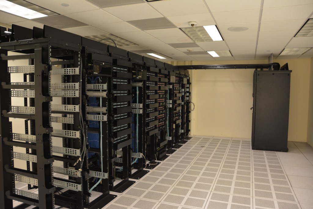
The physical memory does not need to move. The assignment changes through the fabric.
This is the beginning of memory composability.
The rack can contain memory resources that are not permanently mapped to one server for their entire lifetime.
A fabric manager can inventory those resources and control allocation.
The platform becomes able to compose a host with the amount of memory it needs for the current workload.
Pooling and Sharing Are Not the Same Thing
CXL makes an important distinction between memory pooling and memory sharing.
Pooling means memory capacity can be assigned among hosts.
A particular region can be allocated to one host and later reassigned to another.
Sharing goes further.
CXL 3.0 added coherent memory sharing across multiple hosts.
The same memory region can be accessible by more than one host while hardware coherency keeps the views synchronized.
That changes the programming model.
The hosts are no longer only taking turns using a memory resource. They can participate in a shared-memory structure.
The CXL 3.0 white paper describes this as a way to build clusters that work through shared-memory constructs.
That feature existed before CXL 4.0.
CXL 4.0 builds on that fabric foundation rather than introducing shared memory for the first time.
A Fabric Manager Turns Memory Into an Allocatable Resource
The fabric manager is one of the architectural pieces behind composability.
It can discover devices.
Track available capacity.
Configure switches.
Create logical-device assignments.
Modify those assignments as the platform changes.
The role resembles resource orchestration elsewhere in the data center.
A virtualization platform assigns CPUs. A storage system assigns volumes. A network controller assigns connectivity.
A CXL fabric manager can participate in assigning memory resources.
That does not mean every deployment automatically reallocates memory continuously.
The operating model depends on the platform.
The important capability is that the standard defines mechanisms for treating attached memory as something the infrastructure can manage rather than only something fixed at server assembly time.
CXL 3.0 Extended the Fabric Beyond a Single Switch
CXL 3.0 expanded the topology model.
Earlier CXL switching already enabled fan-out from a host to several devices.
CXL 3.0 added richer fabric capabilities, including multi-level switching, peer-to-peer communication and more advanced memory pooling and sharing.
The Consortium describes the direction as dynamically composable systems.
That means a CXL fabric can connect multiple compute domains and multiple devices rather than remaining a simple one-host-to-one-device link.
The topology can contain switches and shared resources.
Hosts can access memory through that fabric.
Devices can also participate in peer-to-peer flows defined by the standard.
This is the architecture CXL 4.0 inherits.
The new generation increases link capability while keeping the fabric model established in the 3.x generation.
CXL 4.0 Doubles the Link Rate to 128 GT/s
The most visible CXL 4.0 change is speed.
CXL 3.x operates up to 64 GT/s.
CXL 4.0 doubles the maximum link rate to 128 GT/s.
The specification is based on PCIe 7.0 electrical technology and retains PAM4 signaling.
The CXL Consortium says the new generation keeps the 256-byte Flit architecture introduced with the 3.x protocol enhancements.
The faster link matters for memory because memory traffic is bandwidth-sensitive.
A processor can generate many reads and writes in parallel.
Accelerators can move large working sets.
Shared-memory systems can create traffic across several hosts.
A faster physical link gives the fabric more transport capacity for those transactions.
The exact application performance still depends on the complete design, workload, topology and traffic pattern.
But the interconnect ceiling has doubled.
Native x2 Width Creates Another Way to Increase Fabric Fan-Out
CXL 4.0 also introduces native x2 link width.
That is a small lane count compared with the x8 and x16 widths often associated with high-bandwidth PCIe devices.
Its value is topology flexibility.
A system has a finite number of high-speed SerDes lanes.
If every endpoint requires a wide link, the number of devices that can connect directly is limited.
A native x2 option gives platform designers another way to divide those lanes across more endpoints.
The CXL Consortium explicitly connects the feature with increased fan-out.
That can be useful in architectures where many memory devices or fabric endpoints need connectivity and each endpoint does not require the widest possible link.
The platform can trade per-link width against the number of attached resources.
Four Retimers Extend the Physical Reach of the Fabric
High-speed links become harder to carry across longer electrical paths.
CXL 4.0 supports up to four retimers.
A retimer receives the high-speed signal, recovers it and transmits a refreshed signal into the next channel segment.
This lets a platform extend the physical reach of the connection while preserving the defined link behavior.
The CXL 4.0 Q&A explains that retimers are also the mechanism used to support optical connectivity paths.
For rack-scale and composable systems, physical distance matters.
A memory resource may not sit immediately next to the processor socket.
It may live in another chassis or behind switching infrastructure.
More retimer support gives designers additional placement options while staying inside the CXL link architecture.
Bundled Ports Let Multiple Links Act as One Accelerator Connection
CXL 4.0 introduces bundled ports.
The feature allows multiple physical device ports to be logically aggregated for Type 1 and Type 2 accelerator devices.
From the application perspective, the bundled connection can behave as one accelerator entity even though the bus enumeration still sees the underlying endpoints.
The purpose is additional bandwidth.
Instead of increasing the internal frequency of one datapath, a device can combine multiple CXL links.
The CXL 4.0 white paper describes bundles with at least one full-capability port and optional streamlined ports focused on data movement.
Bundled ports are primarily an accelerator feature rather than a new memory-pooling primitive.
They still matter to the broader resource-sharing story because CXL is connecting both memory and heterogeneous compute through the same coherent fabric architecture.
Memory RAS Becomes More Important as Memory Moves Into the Fabric
When memory becomes a shared infrastructure resource, maintenance has to become part of the protocol.
CXL 4.0 adds memory RAS enhancements.
RAS stands for reliability, availability and serviceability.
The 4.0 specification adds mechanisms around memory-error visibility and maintenance operations.
The revision history includes additional control for patrol-scrub behavior, host-initiated post-package repair operations at device boot and memory-sparing maintenance operations.
These are infrastructure features.
They do not change the basic load/store programming model.
They help the platform inspect, maintain and manage memory devices that may be serving important workloads through the fabric.
As memory moves away from being only a set of local DIMMs inside one server, the management model has to move with it.
Backward Compatibility Keeps Earlier CXL Generations in the Architecture
CXL 4.0 maintains backward compatibility with CXL 3.x, 2.0, 1.1 and 1.0.
That matters because data-center interconnect generations do not arrive everywhere at the same time.
A new host may support CXL 4.0.
An installed memory device may use an earlier generation.
A switch platform may have a different capability set.
Backward compatibility lets the ecosystem evolve in stages.
The new 128 GT/s rate is available where both ends support it.
Earlier devices can continue operating at their supported rates and feature levels.
The memory-sharing direction therefore does not require every component to be replaced simultaneously.
CXL 4.0 extends the fabric while retaining the architecture built across earlier versions.
Shared Memory Changes How a Rack Can Be Composed
The deeper change is not the link speed.
It is the resource model.
A rack can contain CPUs.
Accelerators.
Local DRAM.
CXL memory expanders.
CXL switches.
Fabric management.
Instead of sizing every server as a permanently fixed island, the infrastructure can create different combinations of resources.
A memory-heavy workload can receive additional pooled capacity.
Another host can receive that capacity later.
A shared-memory design can expose one coherent region to several participating hosts where the system architecture supports it.
The rack begins to look less like a row of identical independent servers and more like a set of resources connected through fabrics.
Compute remains attached to processors.
Memory remains physical memory.
The change is how permanently those resources have to be bound to each other.
CXL 4.0 Is Extending the Path Toward Composable Memory
CXL 4.0 does not invent pooled or shared memory.
CXL 2.0 introduced pooling.
CXL 3.0 added coherent sharing and richer fabric capabilities.
CXL 4.0 gives that architecture more bandwidth, more physical reach, new link-width options, bundled accelerator connectivity and stronger memory-maintenance mechanisms.
That is why the 4.0 generation matters.
The standard is moving from the idea of memory expansion toward a mature fabric where memory can be treated as infrastructure.
A server can still use local DIMMs.
A CXL device can add capacity.
A fabric can pool memory.
Multiple hosts can participate in coherent shared-memory designs.
A fabric manager can control allocation.
RAS mechanisms can maintain the memory resource.
The physical RAM still exists somewhere.
What changes is the boundary around ownership.
Memory is becoming something the system can compose.
That is the upgrade.
Closed-Loop Liquid Cooling Is Becoming Part of the AI Compute Stack
AI infrastructure is usually described through processors, memory and networks.
Cooling is now moving into the same architectural conversation.
Meta’s newest AI-optimized data centers use direct-to-chip closed-loop liquid cooling as part of the facility design. The coolant moves heat away from high-density compute hardware, passes through heat exchangers and then returns to the racks in a continuous loop.
That makes the cooling system part of the compute platform rather than a separate room-level utility.
A GPU rack has a power envelope.
That power becomes heat.
The cold plates, coolant flow, pumps, heat exchangers and external heat-rejection system have to be sized around that heat before the rack can operate at its intended density.
Meta described this shift in detail on August 27, 2026.
The company uses a water-and-glycol coolant mixture in closed loops and says the same coolant can remain in service for up to a decade.
The important change is architectural.
Compute density now influences plumbing design.
Plumbing design influences rack layout.
Rack layout influences the building.
Cooling has become another layer of the AI stack.
Power Density Connects Compute Design Directly to Thermal Design
Every watt consumed by a processor eventually becomes heat that has to leave the system.
That relationship becomes more visible as AI racks concentrate larger amounts of compute into a small physical area.
Meta’s infrastructure team previously described a six-rack pod in which two compute racks contained 72 NVIDIA Blackwell GPUs and consumed about 140 kilowatts.
The surrounding pod used four Air-Assisted Liquid Cooling racks to support that deployment in a traditional data-center environment.
The example shows how thermal architecture follows compute density.
The GPUs define the workload capacity.
Power delivery supplies the electrical energy.
The cooling system removes the resulting heat.
Networking keeps the accelerators connected.
All four systems have to fit into the same physical design.
That is why cooling is becoming a first-order infrastructure parameter.
A data-center team planning a new AI system cannot choose compute density first and treat heat removal as an unrelated decision later.
The two are connected from the beginning.
Direct-to-Chip Cooling Moves the Thermal Path Closer to the Processor
Direct-to-chip liquid cooling shortens the thermal path.
A cold plate sits directly on a high-power component such as a CPU or GPU.
Heat moves from the silicon package into the cold plate.
Liquid flowing through channels inside that plate carries the heat away.
The coolant then moves through the rack-level or facility-level loop toward a heat exchanger.
This is different from cooling only the surrounding room air.
The liquid interacts with the component through a dedicated thermal interface.
The Open Compute Project’s Cold Plate Sub-Project describes direct liquid cooling as an ecosystem extending from the cold plate through the technology cooling system and coolant distribution unit.
That framing is useful because the cold plate is only the first piece.
Tubing, quick disconnects, manifolds, pumps, sensors, filtration, coolant chemistry and heat exchangers all become part of the same thermal path.
The cooling architecture therefore begins on the processor and continues through the rack and the facility.
Meta Uses a Water-and-Glycol Coolant in a Sealed Loop
Meta describes its current closed-loop design as circulating a mixture of water and glycol.
The coolant repeatedly travels through the compute equipment, absorbs heat and then moves toward the heat-exchange stage.
After the heat is transferred away, the cooled liquid returns to the racks.
The same fluid circulates again.
That is the meaning of the closed loop.
The coolant is not continuously consumed as part of the ordinary thermal cycle.
Meta says it expects the coolant used in these loops to remain in service for up to ten years before replacement.
The glycol component gives the fluid system properties suitable for long-term thermal operation, including protection across environmental conditions.
The exact coolant formulation and facility design can vary.
The important architectural feature is recirculation.
The thermal loop carries energy away from the chips while the working fluid remains inside the system.
Heat Exchangers Separate the Compute Loop From Heat Rejection
The coolant has to release the heat it collected from the processors.
That happens through heat exchangers.
A heat exchanger allows thermal energy to move from one fluid or system to another without requiring the two circuits to become one shared loop.
This creates a useful boundary.
The technology cooling system can circulate coolant through the racks.
The facility side can then move that heat toward dry coolers or another site-specific heat-rejection system.
Meta’s typical new data-center design uses direct-to-chip closed-loop cooling with dry coolers where local conditions support that approach.
The coolant therefore handles the internal transport.
The heat exchanger hands the thermal load to the facility.
The dry cooler rejects the heat to the outside environment.
This layered structure keeps the processor-side thermal loop and the larger building system connected while allowing each part to perform a different job.
Dry Coolers Let the Facility Reject Heat Without Consuming the Rack Coolant
Meta says many of its closed-loop sites use dry coolers.
A dry cooler moves outdoor air across heat-exchange surfaces to remove energy from the closed liquid system.
The rack coolant stays inside the loop.
The outside air does not mix with it.
Meta’s water-stewardship documentation says its typical direct-to-chip closed-loop design with dry coolers has no operational water use in the cooling system itself, with site water use limited to other facility needs such as domestic use, cleaning and fire protection.
That statement applies to the specific design Meta describes.
Other data centers can use different cooling architectures depending on climate, site resources and equipment.
The important point for the AI compute stack is that heat rejection can be designed as a separate facility stage.
The chips transfer heat to coolant.
The coolant transfers heat through the exchanger.
The facility rejects that heat outdoors.
Each layer has its own interface.
Cold Plates Are Becoming a Standardized Hardware Interface
As direct-to-chip cooling becomes more common, the industry is also standardizing the components that connect to the processors.
The Open Compute Project’s Cold Plate Sub-Project is developing specifications and guidelines for direct liquid cooling.
Its work covers cold plates, connectors, hose routing, coolant loops and coolant distribution systems.
The project describes its goal as enabling an open ecosystem for direct liquid cooling.
That matters because cooling hardware is beginning to look more like the rest of data-center infrastructure.
Interfaces can be specified.
Flow requirements can be documented.
Connector designs can be standardized.
Coolant compatibility can be tested.
A server vendor, cooling supplier and data-center operator can then design around a shared set of engineering expectations.
Thermal infrastructure becomes a platform with interfaces, not only custom plumbing built independently for each deployment.
Coolant Distribution Units Manage Flow Between the Facility and the Rack
A Coolant Distribution Unit, or CDU, is another important layer.
The CDU manages the liquid flow serving the IT equipment.
Depending on the design, it can contain pumps, heat exchangers, sensors, filtration and control hardware.
The facility side supplies one thermal condition.
The CDU creates the controlled loop needed by the rack.
The rack manifold then distributes coolant to individual servers or cold plates.
This gives operators another boundary in the cooling architecture.
Facility water or facility heat-rejection equipment does not need to connect directly to every processor cold plate.
The CDU can isolate and manage the technology cooling system in between.
Open Compute Project specifications treat the CDU as part of the direct-liquid-cooling ecosystem.
That makes it similar to a power-distribution layer.
Electric power moves through conversion and distribution stages before it reaches the processor.
Cooling can now move through heat-exchange and distribution stages before it reaches the same processor.
Air-Assisted Liquid Cooling Lets Liquid-Cooled Hardware Enter Existing Facilities
Not every data center was originally built with facility liquid loops.
Meta uses Air-Assisted Liquid Cooling, or AALC, for some of those environments.
AALC places pumps and heat exchangers near the racks.
The liquid loop cools the high-density hardware.
The AALC system then transfers the heat into the facility’s existing air-based environment.
This creates a bridge between newer liquid-cooled equipment and buildings designed around a different thermal architecture.
Meta used AALC with its Blackwell deployment in traditional data centers and has described it as a smaller, distributed version of the closed-loop concept.
The core thermal idea remains the same.
Liquid collects heat close to the processors.
A heat exchanger moves that energy into the next cooling stage.
The difference is where that transfer happens.
This lets cooling architecture evolve in stages instead of requiring every facility to use exactly the same building-level loop.
Cooling Capacity Influences How Much Compute Fits Into a Rack
Thermal design also changes physical density.
Meta says cooling the same high-density AI hardware entirely through larger air-handling structures could require substantially more tray space in the example it describes.
Liquid cooling moves much of the thermal transport into cold plates and tubing.
That can leave more of the rack volume available for compute, memory, networking and power hardware.
The relationship is simple.
A rack has finite dimensions.
Every fan, heat sink, duct, manifold and cable consumes space.
The cooling method changes how that space is allocated.
As AI hardware concentrates more electrical power per rack, thermal hardware becomes part of the density equation.
Compute density is therefore not only a semiconductor metric.
It is a mechanical and facility metric too.
The number of accelerators that can operate in one rack depends on whether the rack can receive enough power and remove enough heat.
Cooling Loops Are Designed for Long Service Life
A data-center cooling loop is infrastructure, not a disposable accessory.
It has to operate continuously across long deployment cycles.
Meta says the water-and-glycol mixture in its closed-loop system is expected to remain in service for up to a decade.
Open Compute Project work on direct-to-chip cooling also includes coolant chemistry, corrosion, material compatibility, filtration, connectors and long-term loop requirements.
Those subjects matter because the cooling fluid touches metals, seals, hoses and heat-exchange surfaces across the system.
The thermal performance of the loop has to remain predictable over time.
The mechanical interfaces also have to support maintenance and replacement of IT equipment.
This creates a lifecycle engineering problem.
A GPU generation may change quickly.
The cooling infrastructure around it is expected to support several equipment cycles.
That gives thermal standards another role: help make the rack and facility useful across successive generations of compute hardware.
Cooling Operations Are Becoming Sensor-Driven
A closed-loop system is also a control system.
Operators can measure coolant temperature.
Flow rate.
Pressure.
Rack inlet and outlet conditions.
Heat-exchanger behavior.
Pump state.
Server load.
Outside weather.
Those measurements can be used to change cooling operation dynamically.
The workload is not constant.
Training jobs can move.
Inference traffic can rise and fall.
Outdoor temperature changes through the day and across seasons.
The cooling system therefore has to respond to changing thermal demand.
This makes data-center cooling increasingly similar to other automated infrastructure.
Sensors provide state.
Controllers choose operating points.
The facility changes fan speeds, pump behavior or other control settings.
Cooling becomes software-addressable infrastructure built around a physical thermal loop.
Meta Is Using Reinforcement Learning to Optimize Cooling Control
Meta is also applying AI to the operation of its cooling systems.
The company says its engineering teams built a physics-based simulator that models weather conditions, server load and cooling-equipment behavior.
A reinforcement-learning system can test control decisions inside that simulated environment before policies are applied to the real facility.
Meta says the approach has been scaled to air-cooled data centers in its fleet.
In one pilot, Meta reports that the reinforcement-learning approach reduced supply-fan energy consumption by an average of 20 percent while reducing water usage by 4 percent across varying weather conditions.
Those are Meta’s pilot results for the specific facility and control system it tested.
The architectural point is broader.
Cooling is no longer only a fixed mechanical design.
Its operating policy can also be optimized by software.
The AI compute stack produces heat.
AI can then participate in controlling the infrastructure that removes that heat.
Liquid Cooling Is Becoming an Industry Standards Problem
The move toward higher-density liquid cooling is larger than one data-center operator.
The Open Compute Project and ASHRAE formed an alliance in 2025 focused on liquid-cooling standards and best practices for AI data centers.
Their joint scope spans facility water systems, technology cooling systems, direct-to-chip equipment, immersion cooling and coolant distribution units.
That is a sign that thermal management is becoming an interoperable infrastructure discipline.
Facilities need terminology.
Equipment classes.
Temperature ranges.
Flow requirements.
Connector definitions.
Fluid guidance.
Testing methods.
As those elements become standardized, AI hardware vendors and data-center operators can design around shared thermal interfaces.
Cooling starts to resemble power and networking.
It becomes a layer that needs formal specifications because many independent systems have to connect to it.
New AI Data Centers Are Being Designed Around Liquid Cooling From the Beginning
Meta’s infrastructure plans show the difference between adaptation and native design.
Traditional facilities can use Air-Assisted Liquid Cooling to support newer equipment.
New AI-optimized facilities can include direct-to-chip closed loops in the original building architecture.
That changes planning.
Pipe routing is designed with the data hall.
Heat exchangers are sized with the compute plan.
Dry coolers are selected with the local climate.
Rack density is coordinated with power delivery.
Mechanical systems are designed around the expected thermal load.
Meta says it chooses cooling technologies based on local conditions, including climate, resource availability and technical requirements.
The result is not one identical cooling design for every site.
It is a facility architecture where cooling is chosen alongside compute rather than added after the compute platform is finalized.
The AI Compute Stack Now Extends From Silicon to Heat Rejection
The modern AI stack can be traced through several physical layers.
The model runs on accelerators.
Memory feeds the accelerators.
Networks connect them.
Power systems deliver electrical energy.
Cold plates collect the resulting heat.
Coolant carries that heat through the rack.
CDUs and heat exchangers move it into the facility system.
Dry coolers or other site-specific infrastructure reject it to the environment.
Sensors measure the system.
Control software adjusts operation.
Meta’s closed-loop deployments show how those layers now have to be designed together.
The cooling system is not separate from compute capacity.
It helps define the compute capacity that can operate in a given rack and building.
That is why closed-loop liquid cooling is becoming part of the AI compute stack.
The processor creates the work.
The thermal system makes sustained operation possible.
The two are now designed as one infrastructure problem.
That is the upgrade.
Windows on Arm Is Becoming a Multi-Silicon Platform
Windows on Arm is changing in a specific way.
For several years, the modern Windows on Arm PC story was closely associated with Qualcomm Snapdragon processors.
That is no longer the whole platform.
Microsoft says NVIDIA RTX Spark is joining the Windows on Arm silicon family, with systems planned from Microsoft Surface, ASUS, Dell, HP, Lenovo and MSI in fall 2026.
That creates a broader hardware map.
Snapdragon X continues to power a large group of Copilot+ PCs.
RTX Spark adds another Arm-based Windows platform with a different CPU, GPU, memory and software stack.
The operating system stays Windows 11 on Arm.
The application architecture stays Arm64.
The silicon underneath can now come from more than one major family.
That is an important platform transition.
Windows on Arm is becoming less about one processor line and more about a common Windows environment that several Arm hardware designs can target.
RTX Spark Adds NVIDIA to the Windows on Arm Silicon Family
Microsoft’s August 25 Windows Developer Blog describes NVIDIA as a new Windows on Arm silicon provider.
The hardware itself was announced earlier in 2026.
RTX Spark combines a 20-core NVIDIA Grace CPU with a Blackwell RTX GPU connected through NVLink-C2C.
NVIDIA says the platform supports up to 128GB of unified memory and up to one petaflop of FP4 AI compute.
Those specifications create a different type of Windows on Arm system from the Snapdragon X laptops that established the current Copilot+ PC generation.
The CPU is still Arm-based.
The operating system is still Windows on Arm.
But the graphics, AI acceleration, memory system and developer stack come from NVIDIA.
That is the architectural point.
Windows does not have to be tied to one Arm implementation.
The same Windows Arm64 platform can sit above a second silicon family with a different balance of CPU, GPU and AI hardware.
Surface, ASUS, Dell, HP, Lenovo and MSI Expand the Hardware Side
A silicon platform becomes more significant when OEMs build systems around it.
Microsoft says RTX Spark devices are planned for fall 2026 from Surface, ASUS, Dell, HP, Lenovo and MSI.
That means the transition is not limited to one reference machine.
Several Windows PC manufacturers are preparing products around the same Arm-based NVIDIA platform.
Microsoft also has a Surface RTX Spark Dev Box aimed at developers.
The Dev Box runs Windows 11 Pro and is preconfigured with development tools such as Visual Studio Code, GitHub Copilot in Windows Terminal, WSL and PowerShell 7.
This creates several layers of hardware choice.
Snapdragon X systems continue to cover thin-and-light Windows on Arm PCs.
RTX Spark adds systems aimed at local AI, creation, graphics and development workloads.
The same Windows architecture can now appear across different product designs.
That is how an operating-system platform grows beyond the identity of one chip vendor.
The Common Layer Is Windows Arm64
The shared technical layer is Arm64 Windows.
Application developers do not write one Windows program for Snapdragon and a completely different operating system target for RTX Spark.
They target Windows on Arm.
Microsoft’s current Windows on Arm documentation describes several application paths.
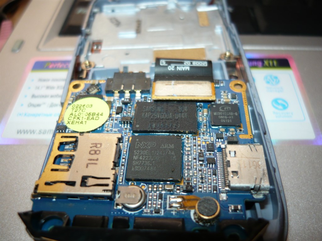
A developer can build a native Arm64 application.
An existing x86 or x64 application can run through Windows emulation.
A developer can also use Arm64EC, an ABI that allows Arm-native and emulated x64 code to coexist within the same process.
Those software paths sit above the processor family.
The silicon underneath can change.
The operating-system application model remains consistent.
That is what makes multiple silicon providers useful to a platform.
Hardware vendors can differentiate below Windows.
Developers can continue targeting the Windows Arm64 environment above it.
Native Arm64 Apps Run Directly on the Architecture
The most direct application path is native Arm64.
Microsoft recommends native Arm builds where possible for performance and power efficiency.
The Windows developer stack now includes Arm-native versions of Visual Studio, Visual Studio Code and current .NET tooling.
C and C++ applications can target Arm64.
Modern .NET applications can run natively on Arm64.
Java, Python, Node.js and other development environments also have Arm paths documented by Microsoft.
A native build means the application’s machine code is compiled directly for Arm64 instructions.
Windows loads that code without translating x86 or x64 instructions first.
That model is independent of whether the Windows PC uses Snapdragon X or RTX Spark.
Both expose the Arm64 architecture to Windows.
The exact microarchitecture differs.
The application target remains Arm64.
Prism Keeps x86 and x64 Applications Inside the Same Windows Environment
Windows also supports existing x86 and x64 software through emulation.
Microsoft’s current emulator is Prism.
Prism is included with Windows 11 on Arm and translates blocks of x86 or x64 instructions into Arm64 instructions at runtime.
Windows caches translated blocks so later execution can reuse them.
That gives existing Windows applications a path onto Arm systems without requiring an immediate native rebuild.
Prism is therefore part of the platform transition.
The hardware ecosystem can expand while the software ecosystem continues operating across native and emulated code.
Microsoft notes that some Prism performance features were originally tuned specifically for Snapdragon processors, while Prism itself is available across supported Windows 11 on Arm devices.
As Windows on Arm adds another silicon family, the operating system becomes the layer responsible for carrying this compatibility model across the broader hardware base.
Arm64EC Lets One Process Mix Native Arm Code and x64 Code
Arm64EC adds another migration path.
The name stands for Arm64 Emulation Compatible.
It is an application binary interface for Windows 11 on Arm.
An Arm64EC process can contain code compiled as Arm64EC while also using x64 code that runs under emulation.
That lets developers move an application incrementally.
A CPU-intensive module can be rebuilt first.
Another dependency can remain x64.
More code can be moved later.
The application does not have to transition in one step.
This is especially relevant to large Windows desktop applications with long dependency chains.
The Arm ecosystem can expand while software vendors decide how quickly each part of an application should become native.
Arm64EC therefore acts as a bridge between the existing Windows x64 software world and the growing Arm64 hardware world.
The App Ecosystem Is Growing Alongside the Hardware
Microsoft’s August 2026 update says the Works on Windows on Arm catalog now contains more than 7,000 verified apps and games.
That figure comes from compatibility data used by Microsoft.
The catalog includes software across productivity, development, creative work, STEM, security and entertainment.
Microsoft also points to recent Arm work from vendors such as Google, Adobe, Slack, Trello, Dropbox, Blender, Figma and Camtasia.
The number matters because processor diversity alone does not create a platform.
Users need software.
Developers need tools.
OEMs need demand.
Microsoft describes this as a cycle.
More Arm devices give developers more reason to build or optimize applications.
More applications make the hardware more useful to more users.
As the silicon base expands, the software catalog becomes the common layer connecting those devices.
App Assure Gives Developers a Migration Support Path
Microsoft also operates App Assure for Windows on Arm.
The program includes an Arm Advisory Service for software developers.
Microsoft says the service provides technical guidance, workshops, code samples and escalation paths to Microsoft engineers.
That matters because architecture transitions are not only compiler decisions.
Applications can include plug-ins, drivers, native libraries, installers, JIT runtimes and third-party dependencies.
Moving those pieces to Arm may involve different work.
App Assure gives developers a support channel while Windows on Arm grows.
This is another platform layer that is independent of the specific processor.
A developer porting an application to Arm is targeting Windows.
The resulting application can then participate across Windows Arm64 hardware families as those systems arrive.
RTX Spark Brings the CUDA and RTX Stack Into Windows on Arm
NVIDIA’s entry adds more than a CPU architecture.
RTX Spark brings CUDA, RTX, TensorRT and NVIDIA graphics technologies into an Arm-based Windows PC.
NVIDIA’s TensorRT for RTX 1.6 now lists Windows Arm64 support for RTX Spark.
NVIDIA also documents Windows on Arm support in current video and AI tooling.
That creates a new developer combination.
Windows Arm64 applications can run on an Arm CPU while using an NVIDIA Blackwell GPU and NVIDIA’s acceleration software.
This is a different software stack from the NPU-centered Windows AI path associated with many Snapdragon X Copilot+ PCs.
Both can exist under Windows.
That is what multi-silicon support changes.
The operating system becomes the common application platform.
Each hardware family can then expose its own acceleration capabilities underneath it.
Unified Memory Changes the Shape of Local AI Workloads
RTX Spark also introduces a large unified-memory design into this part of the Windows PC ecosystem.
NVIDIA says RTX Spark systems can support up to 128GB of unified memory.
The Grace CPU and Blackwell GPU share that memory architecture.
That matters for local AI because model size is often constrained by available accelerator memory.
NVIDIA says the platform is designed to run models up to 120 billion parameters locally in supported configurations.
Those are NVIDIA platform claims and depend on model format, precision, software and workload.
The broader architectural point is simpler.
Windows on Arm can now sit above hardware with a very different memory model from earlier mainstream Arm laptops.
That widens the kinds of machines that can belong to the Windows Arm64 family.
Windows on Arm Can Serve Thin-and-Light PCs and Developer Systems
A broader silicon base also expands product categories.
Snapdragon X established Windows on Arm strongly in thin-and-light laptops and Copilot+ PCs.
RTX Spark adds high-memory systems aimed at AI developers, creators and graphics-heavy workloads.
Microsoft’s Surface RTX Spark Dev Box takes that idea into a desktop development device.
NVIDIA also describes RTX Spark laptops and small desktops.
The operating system is therefore stretching across different physical formats and workload profiles.
One Windows on Arm machine can prioritize mobility.
Another can prioritize local model capacity.
Another can act as a developer workstation.
The platform identity becomes the operating system and architecture rather than one device class.
That is another sign that Windows on Arm is becoming a general Windows hardware platform instead of one narrow category.
Developer Tools Are Becoming Native on Arm Too
A hardware ecosystem becomes easier to sustain when developers can build on the same architecture they are targeting.
Microsoft’s current Windows on Arm documentation lists Arm-native Visual Studio and Visual Studio Code.
The .NET SDK supports Arm64.
MSVC includes Arm64 and Arm64EC targets.
Developers can compile, debug and test Arm applications directly on an Arm Windows machine.
RTX Spark adds another Arm-based development platform with NVIDIA’s own compute stack available at the same time.
That means a developer can work inside Windows Arm64 while targeting CPU code, GPU code and local AI workloads.
The development environment is becoming part of the Arm ecosystem rather than depending entirely on cross-compilation from x64 PCs.
Windows Becomes the Stable Layer While Silicon Vendors Differentiate Below It
The most important platform effect is separation.
Microsoft owns Windows.
Qualcomm designs Snapdragon X systems.
NVIDIA designs RTX Spark with its Grace CPU and Blackwell GPU architecture.
OEMs choose how those platforms become laptops, desktops and developer devices.
Application developers target Windows Arm64.
That creates a stable layer above changing hardware.
The processor vendors can compete through CPU design, GPU architecture, AI acceleration, memory systems and power characteristics.
Windows can expose those capabilities through its operating-system APIs and driver model.
Applications can choose native Arm64, Arm64EC or emulation paths.
This is the same basic pattern that has long made Windows flexible across different x86 PC designs.
Windows on Arm is beginning to gain more of that hardware diversity.
More Silicon Families Can Strengthen the Software Incentive
More hardware families can also change the economics of software support.
A developer considering an Arm-native build is not targeting only one processor line if several Windows hardware families use the same application architecture.
The addressable Windows Arm64 ecosystem becomes broader.
That can make native compilation, testing and optimization useful across more devices.
Microsoft’s August app-ecosystem update connects these two trends directly.
More hardware vendors and OEMs are entering the platform.
The Arm app catalog is expanding at the same time.
The relationship is important.
Software makes hardware more useful.
Hardware gives software developers more users to reach.
The platform grows when both sides reinforce each other.
Windows on Arm Is Expanding Beyond a Single Silicon Family
Windows on Arm now has a clearer platform structure.
Snapdragon X remains a major Arm Windows family.
RTX Spark adds NVIDIA Grace and Blackwell hardware to the same operating-system architecture.
Surface, ASUS, Dell, HP, Lenovo and MSI are preparing systems.
Windows supports native Arm64 applications.
Prism keeps x86 and x64 applications available through emulation.
Arm64EC lets developers mix native Arm code with existing x64 code during migration.
Microsoft says the verified app catalog has passed 7,000 applications and games.
Developer tools themselves are increasingly native on Arm.
NVIDIA adds CUDA, RTX and TensorRT to Windows Arm64 on its hardware.
The result is not one processor replacing another.
It is Windows gaining more Arm hardware underneath the same application platform.
That is what changes when an architecture becomes an ecosystem.
The operating system stays stable.
The silicon choices multiply.
That is the upgrade.
Ray Reconstruction Works Inside the Rendered Frame
Ray Reconstruction belongs to a different part of the graphics pipeline than Frame Generation. Frame Generation changes how many frames are presented. Ray Reconstruction changes how a ray-traced frame itself is rebuilt.
A real-time ray tracer cannot sample every possible light path for every pixel. It traces a limited number of rays, producing useful but incomplete lighting information. A reconstruction stage then turns those samples into the image the player sees.
NVIDIA released DLSS 4.5 Ray Reconstruction on August 25, 2026. NVIDIA describes it as a neural rendering technique for ray-traced and path-traced games that replaces hand-tuned denoisers with a supercomputer-trained AI network. The model uses noisy ray-traced input together with temporal and spatial engine data.
That places the AI model inside the renderer. It is not merely adding a later presentation frame. It participates in deciding how sampled light becomes the finished rendered frame.
Real-Time Ray Tracing Begins With Limited Samples
Ray tracing follows rays through a scene to calculate intersections, materials, reflections, shadows and lighting. Path tracing extends the idea across more light bounces.
Offline rendering can spend a long time sampling a frame. Real-time games have milliseconds. At 60 FPS, a frame has about 16.7 milliseconds. At 120 FPS, it has about 8.3 milliseconds.
The renderer therefore works from a limited sample budget. Some pixels receive direct ray information. Other information has to be inferred from neighboring pixels, earlier frames and structured data from the engine.
This is the reconstruction problem. The renderer does not need every final pixel to be directly sampled if the reconstruction stage has enough evidence to estimate the missing information.
Ray Reconstruction is designed around that relationship. Ray tracing provides samples. The engine provides structure. The neural model reconstructs the output.
Denoising and Super Resolution Are Becoming One Reconstruction Path
A conventional real-time ray-traced pipeline can contain separate operations. The ray tracer generates noisy lighting buffers. Denoisers process ray-traced effects. A temporal upscaler then reconstructs a higher-resolution output.
NVIDIA introduced Ray Reconstruction with DLSS 3.5 to replace multiple hand-tuned denoisers with one neural network. NVIDIA now describes Ray Reconstruction as unified with DLSS Super Resolution.
The practical result is a different pipeline boundary. The model can work from noisy ray-traced information and engine data while also participating in the reconstruction of the final high-resolution frame.
That gives the AI stage access to information before it has been reduced to a finished lower-resolution image. The reconstruction model can reason over the ray-traced samples themselves while building the output.
Ray Reconstruction is therefore more than a post-process denoiser. It sits where denoising, temporal reconstruction and high-resolution image formation meet.
The Model Receives Structured Engine Buffers
Ray Reconstruction does not receive only a noisy color image.
NVIDIA’s Streamline programming guide lists several required or supported resources. These include diffuse albedo, specular albedo, surface normals, roughness, depth, motion vectors and noisy ray-traced color. Specular motion information can also be supplied.
Those buffers explain the scene.
Albedo describes material reflectance. Normals describe surface orientation. Roughness helps explain how reflections spread. Depth identifies geometry relationships. Motion vectors describe movement between frames. The noisy color buffer contains the sampled ray-traced lighting.
Together, these signals give the model more context than a finished screenshot provides.
That is why Ray Reconstruction belongs inside the rendering pipeline. It uses data that comes directly from the game engine and renderer before final presentation. The model is reconstructing with information about materials, geometry, motion and sampled light.
Temporal Data Connects the Current Frame to Earlier Frames
Real-time reconstruction can reuse information across time.
A reflection may be sampled differently from one frame to the next. A lighting detail may appear in several temporal samples. A moving object changes position, but motion vectors describe how that movement occurred.
Ray Reconstruction can use those relationships while deciding what information should contribute to the current frame.
NVIDIA says DLSS 4.5 uses temporal and spatial engine data and gives developers finer control over temporal accumulation. That means the reconstruction stage can be tuned around how history contributes to the result.
The previous frame is not simply discarded once a new frame begins. It becomes another source of evidence.
This turns reconstruction into a temporal rendering process. The model does not only ask what the current noisy samples contain. It also considers how the scene has evolved across recent frames.
Spatial Data Helps the Model Respect Scene Structure
Spatial reconstruction is the other half of the problem.
Nearby pixels may belong to the same surface, or they may sit on opposite sides of a geometry edge. They may use different materials. They may contain different lighting behavior.
A reconstruction model therefore needs to decide which nearby information can be shared and which boundaries should stay distinct.
NVIDIA says the second-generation Ray Reconstruction model has deeper spatial awareness and uses engine pixel sampling and motion data more intelligently.
Normals, roughness, albedo and depth help define that structure. They give the model signals that describe whether two neighboring pixels belong to similar or different parts of the scene.
The reconstruction stage is therefore not simply smoothing noisy pixels. It is deciding how ray-traced information should be distributed across geometry and materials while the final image is built.
DLSS 4.5 Adds a Second-Generation Transformer Model
The August 2026 release moves Ray Reconstruction to a second-generation transformer model.
NVIDIA says the new model delivers 35 percent more compute capability and processes 20 percent more parameters while maintaining similar performance to the previous Ray Reconstruction model.
Those figures are NVIDIA’s published model-design measurements.
NVIDIA also says the model was trained on a larger dataset and uses that additional capacity to improve lighting reconstruction, temporal stability and clarity in motion.
Training data matters because the network has to learn how sparse ray-traced samples relate to reference images across many scene types, materials, movements and lighting conditions.
The deployed model then performs that reconstruction in real time on RTX Tensor Cores.
The model can evolve while the game renderer continues providing the same general classes of structured inputs.
Ray Reconstruction Can Work With Ray Tracing and Path Tracing
NVIDIA positions Ray Reconstruction for both ray-traced and path-traced scenes.
A ray-traced game may use rays selectively for reflections, shadows or global illumination. A path-traced renderer can push much more of the scene’s lighting through ray-based transport.
Both create a reconstruction task because the renderer still has a finite number of samples available for each frame.
As more of the image depends on path-traced lighting, the reconstruction stage becomes more central. It can participate in the appearance of a large part of the scene rather than one isolated effect.
That is why Ray Reconstruction has a different role from a conventional graphics setting. It can become part of the lighting pipeline itself.
The renderer produces sampled light. The reconstruction model turns those samples into the image that moves forward through the frame pipeline.
Ray Reconstruction and Frame Generation Solve Different Problems
DLSS now contains several neural rendering technologies that operate at different stages.
Super Resolution reconstructs a higher-resolution frame from a lower-resolution input.
Ray Reconstruction reconstructs ray-traced lighting and the high-resolution image using sampled rays and engine data.
Frame Generation creates additional presentation frames between rendered frames.
Multi Frame Generation can create several presentation frames around rendered frames.
These technologies can be combined, but they are not interchangeable.
A game can use Ray Reconstruction to build each rendered frame and then use Frame Generation later to increase the presentation rate.
That is also why this topic is separate from the FPS article.
Ray Reconstruction changes the internal construction of the rendered frame.
Frame Generation changes the number of frames sent through the presentation pipeline.
One is an image reconstruction layer. The other is a frame presentation layer.
Ray Reconstruction Runs Across GeForce RTX Generations
NVIDIA says DLSS Ray Reconstruction is available across GeForce RTX GPUs.
That includes RTX generations that do not support the highest Multi Frame Generation modes.
Ray Reconstruction uses RTX Tensor Core hardware to execute the neural model.
The important architectural point is that the model generation and GPU generation are separate concepts.
A GPU can stay physically unchanged while NVIDIA updates the reconstruction network through later DLSS releases.
DLSS 4.5 demonstrates that model-driven graphics features can continue evolving in software.
The renderer still supplies the required buffers.
The Tensor Cores execute the newer network.
The output changes because the neural model changed.
That gives neural rendering a software-like upgrade path inside a hardware-accelerated graphics pipeline.
Streamline Makes Ray Reconstruction an Engine Integration
For developers, Ray Reconstruction appears as a feature in NVIDIA Streamline.
The current programming guide shows the application tagging the required buffers, configuring DLSS options and invoking the Ray Reconstruction feature during rendering.
The game supplies the scene resources. Streamline connects them to the DLSS plugin. The model evaluates the frame at the appropriate point in the renderer.
This integration detail matters.
Ray Reconstruction is not a generic image filter attached after a completed frame. The engine has to provide compatible buffers at the correct resolution, format and timing.
Motion vectors need to represent camera and object movement. Surface information has to match the scene. The noisy ray-traced input has to be available before final reconstruction.
The engine therefore participates directly in the AI rendering stage.
Unreal Engine Gives the Feature a Reusable Production Path
NVIDIA distributes DLSS 4.5 through its Unreal Engine plugin.
The current NVIDIA developer page lists support for Unreal Engine 5.5 through 5.8 and exposes Ray Reconstruction alongside Super Resolution, DLAA, Reflex and frame-generation features.
That gives developers a reusable integration path.
A project still has to configure the rendering pipeline correctly and provide the required inputs, but the plugin packages the connection to NVIDIA’s DLSS stack inside the engine workflow.
This is part of what makes Ray Reconstruction a rendering layer rather than a single-title experiment.
It has SDK documentation, Streamline support and an engine integration path.
The same basic neural reconstruction stage can therefore appear across different games while each project keeps its own art, materials, geometry and ray-tracing setup.
RTX Remix Extends the Same Layer Into Remastering
NVIDIA also added DLSS 4.5 Ray Reconstruction to RTX Remix in August 2026.
RTX Remix is a modding platform that can add modern ray-traced and path-traced rendering to older PC games.
That creates another type of integration.
A game that was not originally designed around modern path tracing can receive a new rendering layer through the Remix workflow. Ray Reconstruction can then process the sampled lighting inside that updated renderer.
NVIDIA announced the feature alongside new and updated RTX Remix projects including Painkiller RTX and The Elder Scrolls III: Morrowind RTX.
The individual titles are examples. The larger point is portability.
The same neural reconstruction model can participate in newly developed games and in remastering workflows built around a different renderer.
New Games Are Treating Ray Reconstruction as a Graphics Layer
NVIDIA’s Gamescom 2026 announcements show Ray Reconstruction moving into current game integrations.
The company says 007 First Light is scheduled to receive a path-tracing and DLSS 4.5 Ray Reconstruction update on September 15, 2026. NVIDIA also demonstrated CONTROL Resonant with path tracing and DLSS 4.5.
These announcements show how the technology fits into a modular graphics stack.
Ray tracing or path tracing provides lighting samples.
Ray Reconstruction rebuilds the sampled lighting and high-resolution image.
Frame Generation can operate later if the game uses it.
The display receives the resulting presentation stream.
Each stage solves a different problem.
That modularity is important because it gives developers separate controls over rendering, reconstruction and presentation rather than treating the whole DLSS stack as one indivisible feature.
Neural Rendering Is Moving Deeper Into the Renderer
AI graphics once appeared easiest to understand near the end of the pipeline.
Upscale the image.
Generate another frame.
Apply an enhancement after rendering.
Ray Reconstruction moves the neural model deeper.
It receives material information, depth, motion, geometry-related buffers and noisy ray-traced lighting.
That means the model participates in a stage that previously depended on conventional denoising and temporal reconstruction algorithms.
The AI is not only processing a finished picture.
It helps determine what the finished ray-traced picture should be.
The engine generates structured signals. The model combines them. The result moves forward to the rest of the graphics pipeline.
This is why neural rendering increasingly looks like part of the renderer itself rather than a feature placed on top of it.
Ray Reconstruction Is Becoming Its Own Layer of Real-Time Rendering
DLSS 4.5 makes the architecture easy to separate.
Real-time ray tracing produces limited samples.
The game engine provides noisy ray-traced color, motion vectors, depth, normals, roughness and material information.
Ray Reconstruction processes those signals through a second-generation transformer model.
The model combines temporal and spatial evidence and reconstructs the image.
Frame Generation can then operate later in the pipeline if enabled.
Those stages are distinct.
Ray Reconstruction is not another name for Frame Generation. It is not simply a label for resolution scaling. It is a neural reconstruction stage built around ray-traced and path-traced data.
NVIDIA’s August 2026 release adds the new transformer model and brings it into current DLSS integrations, RTX Remix and new game announcements.
Real-time rendering is becoming a combination of sampled physics and learned reconstruction.
The rays provide evidence.
The engine provides structure.
The neural model rebuilds the image.
That is the upgrade.
FPS Now Describes More Than One Stage of the Graphics Pipeline
Frames per second used to be a relatively direct measurement.
The game engine rendered a frame.
The GPU finished it.
The display received it.
Count how many completed game frames were produced in one second and the result was FPS.
Frame generation adds another stage.
A modern rendering pipeline can produce traditionally rendered frames and then synthesize additional frames between them before presentation.
That means two frame rates can exist at the same time.
One describes how often the game and GPU produce new rendered frames.
Another describes how many total frames reach the display after frame generation is applied.
Both numbers are useful.
They describe different parts of the pipeline.
NVIDIA DLSS, AMD FSR and Intel XeSS now all include frame-generation technologies. NVIDIA and Intel have extended the idea into multi-frame generation, where several generated frames can be inserted around each traditionally rendered frame.
The FPS counter is therefore becoming a presentation metric as well as a rendering metric.
To understand a modern game, the first question is no longer only “How many FPS?”
It is also “Which FPS are we measuring?”
Rendered FPS Still Measures the Game's Native Work Cadence
The base rendered frame rate remains the starting point.
A rendered frame contains a new game state produced through the normal game pipeline.
The CPU advances simulation and game logic.
The engine prepares scene data.
The GPU processes geometry, materials, lighting, ray tracing, post-processing and other rendering work.
When that frame is complete, it represents one newly rendered sample of the game.
If the pipeline produces 60 of those frames every second, the base rendered frame rate is 60 FPS.
That cadence matters because it is tied directly to how frequently the game generates new visual states from simulation and user input.
Frame generation does not remove that cadence.
It adds presentation frames around it.
A system can therefore display a much larger total FPS number while the game itself continues to render at a lower base rate.
This is not a contradiction.
It is a layered pipeline.
Rendered FPS describes one layer.
Generated frames add another.
The distinction becomes increasingly important as multi-frame generation raises the ratio between the two.
Generated Frames Add New Presentation Samples Between Rendered Frames
Frame generation works by estimating what an intermediate image should look like between rendered frames.
The exact implementation differs by vendor.
The system can use information such as motion vectors, depth, optical-flow information, previous frames and additional engine data.
The frame-generation model or algorithm then creates a new image positioned between the rendered samples.
That generated frame is real in the sense that it is presented to the display.
It contributes to visible motion.
It is not a duplicate frame.
It contains an estimated intermediate state built from the information available to the frame-generation system.
AMD describes FSR Frame Generation as predicting and inserting new frames between consecutive rendered frames.
Intel describes XeSS Frame Generation as AI-based frame interpolation that produces detailed high-resolution frames.
NVIDIA’s current DLSS Multi Frame Generation goes further by generating several frames from one rendered-frame interval.
The output stream therefore contains a mixture.
Some frames come directly from the conventional game-rendering pipeline.
Others are synthesized for presentation.
The displayed FPS number can count both.
NVIDIA DLSS 4.5 Can Generate Up to Five Frames Per Rendered Frame
NVIDIA’s current DLSS 4.5 makes the difference between rendered and displayed frame rate especially visible.
DLSS 4 introduced Multi Frame Generation for GeForce RTX 50 Series GPUs.
DLSS 4.5 extends that system with 6X Multi Frame Generation and Dynamic Multi Frame Generation.
NVIDIA says its current 6X mode can generate up to five additional frames per rendered frame.
That creates a six-frame output sequence around one traditionally rendered frame in the corresponding multiplier model.
The number shown as output FPS can therefore move much farther away from the underlying rendered-frame cadence than it did with single-frame generation.
This is why a 240 FPS presentation no longer tells the entire rendering story by itself.
The display may be receiving 240 frames every second.
The game engine may be rendering only part of those frames directly.
DLSS fills the rest of the presentation stream with generated frames.
The output FPS still measures how many frames are being presented.
The rendered FPS measures how often the conventional pipeline produces new source frames.
Both are part of the same performance picture.
Dynamic Multi Frame Generation Can Adjust the Multiplier Around a Target
DLSS 4.5 also changes frame generation from a fixed multiplier into a dynamic control system.
NVIDIA’s Dynamic Multi Frame Generation can adjust how many frames are generated during gameplay.
The system can target a desired output frame rate and vary the generation ratio to match changing performance conditions.
That connects frame generation more directly to the display.
A 240Hz monitor has a presentation capacity of 240 refreshes per second.
The game may move above and below one rendered-frame rate as scene complexity changes.
A dynamic frame-generation system can adjust the number of synthesized frames used to fill the presentation stream.
The frame-generation ratio therefore becomes another variable in the graphics pipeline.
Resolution can change through dynamic resolution scaling.
Upscaling quality modes can change the internal rendering resolution.
Frame generation can now change its multiplier.
The performance system is becoming more adaptive.
Displayed FPS becomes the result of several coordinated stages rather than one fixed relationship between the engine and the monitor.
AMD FSR Frame Generation Adds an Intermediate Frame Stream
AMD’s current FSR “Redstone” stack includes FSR Frame Generation alongside FSR Upscaling, Ray Regeneration and Radiance Caching.
AMD says FSR Frame Generation uses machine learning to predict and insert intermediate frames between two consecutively rendered frames.
The frame-generation stage can therefore increase the presentation frame rate while the underlying renderer continues producing the source frames.
AMD’s published Redstone performance examples combine several FSR technologies, so the final multiplier can include more than frame generation alone.
That distinction is useful.
Upscaling changes how the rendered frame is produced.
Frame generation changes how many frames are presented between rendered samples.
Anti-Lag 2 addresses another part of the pipeline: input-to-display responsiveness.
The technologies can work together, but they describe separate operations.
For FPS measurement, FSR Frame Generation creates the same general distinction seen in other modern pipelines.
There is a rendered frame rate.
There is a post-generation output frame rate.
The second can be higher because the presentation stream contains generated frames.
Intel XeSS 3 Extends Frame Generation Into Multi-Frame Generation
Intel has moved in the same direction with XeSS 3.
The XeSS 3 stack includes XeSS Super Resolution, XeSS Multi-Frame Generation and Xe Low Latency.
Intel says XeSS Multi-Frame Generation can insert up to three AI-generated frames between rendered frames on supported Intel hardware.
That moves XeSS beyond the one-generated-frame model used by earlier frame-generation systems.
Intel describes the progression as moving from a 1:1 relationship toward a 3:1 generated-to-rendered ratio for Multi Frame Generation.
The exact output configuration depends on the implementation and selected mode.
The architectural point is the same.
The display stream can contain several AI-generated frames for each rendered-frame interval.
Intel also requires Xe Low Latency as part of XeSS Frame Generation.
That connects the increased presentation rate with a separate latency-management layer.
The result is another example of why one FPS value is becoming incomplete on its own.
The total number of presented frames can be high.
The cadence of rendered game states can be lower.
Latency is measured separately.
All three can be reported together.
Output FPS Measures Presentation Throughput
Once frame generation is active, output FPS becomes a useful term.
Output FPS describes the total rate at which frames are being sent through the final presentation path.
That total can include rendered frames and generated frames.
If a game renders 60 source frames per second and a frame-generation system inserts one intermediate frame between each rendered pair, the display stream can approach a higher presentation rate.
With multi-frame generation, the difference can become larger.
This presentation rate matters because displays have their own refresh capacity.
A 120Hz, 165Hz, 240Hz or 360Hz monitor can show more temporal samples when the graphics pipeline supplies them.
Generated frames can occupy those additional presentation slots.
The motion sequence can therefore become visually denser than the base rendered stream alone.
Output FPS answers a direct question.
How many frames are reaching the presentation stage each second?
Rendered FPS answers another.
How often is the game producing a fully rendered source frame?
Modern frame-generation benchmarking benefits from keeping those two measurements separate.
Latency Remains a Separate Measurement From Output FPS
Frame rate and latency are connected, but they are not the same metric.
FPS measures frame throughput.
Latency measures time.
For gaming, one important latency path begins with an input event and ends when the corresponding visual response reaches the display.
Modern frame-generation systems therefore pair increased presentation rates with dedicated latency technologies.
NVIDIA uses Reflex.
AMD uses Radeon Anti-Lag 2 in supported titles.
Intel uses Xe Low Latency, or XeLL, as a required component of XeSS Frame Generation.
These technologies work on CPU/GPU scheduling and other parts of the pipeline to reduce input-to-display delay.
Their existence shows why latency deserves its own number.
A game can have a high displayed FPS after frame generation while latency remains something that must be measured in milliseconds.
The two metrics describe different properties.
Displayed FPS tells us how dense the presentation stream is.
Latency tells us how long the system takes to reflect an action on screen.
A modern performance profile can include both instead of asking one number to represent the entire experience.
Frame Time Still Explains the Cadence Behind the Rendered Stream
Frame time is another useful measurement.
FPS and frame time describe the same cadence from different directions.
At 60 rendered FPS, each rendered frame has roughly 16.7 milliseconds available on average.
At 120 rendered FPS, that falls to about 8.3 milliseconds.
At 240 rendered FPS, it is about 4.2 milliseconds.
Frame generation can create additional display frames inside the presentation timeline, but the base render frame time still tells us how frequently the game is producing new source frames.
That makes frame time valuable when analyzing a generated-frame pipeline.
A benchmark can show a high output FPS while also reporting the underlying render frame time.
The two values explain the relationship directly.
One tells us how often the source frames are produced.
The other tells us how many total presentation frames are being delivered.
This is especially useful for dynamic multi-frame generation because the output multiplier itself can change while the base rendering workload also changes.
Frame time gives the rendered layer a stable measurement language.
Frame Pacing Determines How Those Frames Are Spaced on the Display
A total FPS count says how many frames appear in one second.
Frame pacing describes how evenly those frames are distributed through that second.
That distinction becomes more relevant when the presentation stream includes generated frames.
A frame-generation system has to place the synthesized frames between rendered samples at appropriate times.
NVIDIA’s Multi Frame Generation architecture includes hardware Flip Metering on GeForce RTX 50 Series GPUs to manage presentation timing.
Intel’s XeSS Frame Generation uses a proxy swapchain interface that handles presentation of rendered and generated frames with pacing logic.
The purpose is temporal placement.
A 240 FPS stream corresponds to an average interval of about 4.17 milliseconds between presented frames.
To create a regular motion sequence, the rendered and generated frames need to arrive across that timeline in a controlled cadence.
Frame pacing therefore becomes another measurement beside FPS.
The total count tells us volume.
The spacing tells us timing consistency.
Modern graphics pipelines increasingly manage both.
The Display Refresh Rate Sets the Capacity of the Final Stage
The monitor remains the final stage.
A 120Hz display can refresh up to 120 times each second.
A 240Hz display has twice that presentation capacity.
A 360Hz display increases it again.
Frame generation gives the GPU another way to populate those refresh opportunities.
That is why current multi-frame-generation systems are often discussed alongside high-refresh monitors.
NVIDIA’s Dynamic Multi Frame Generation is explicitly designed to target a user’s desired output frame rate, including high-refresh 4K gaming scenarios.
Intel positions XeSS Multi-Frame Generation as a way to increase the number of presented frames.
AMD FSR Frame Generation similarly increases the output stream by inserting intermediate frames.
The relationship between GPU and monitor is therefore changing.
A high-refresh panel no longer depends only on the number of traditionally rendered frames the engine can produce.
Generated frames can use part of that display capacity too.
Refresh rate remains a hardware property of the monitor.
Output FPS remains a property of the graphics pipeline.
Frame generation is the stage connecting more of one to the other.
Engine Data Helps Frame Generation Build the Intermediate Image
Generated frames are not created from one screenshot alone.
Modern implementations can receive structured information from the game engine.
Motion vectors describe how pixels or objects are moving between frames.
Depth data describes the spatial relationship between scene elements.
Previous and current rendered frames provide visual history.

Optical-flow or AI-based motion estimation can add another source of movement information.
NVIDIA’s frame-generation systems combine game data with AI inference.
AMD’s FSR Frame Generation uses motion information to predict intermediate frames.
Intel’s XeSS Frame Generation developer interface requires the application to provide resources such as motion vectors and depth.
NVIDIA’s 2026 Enhanced Frame Generation model also uses additional UI buffers in selected game engines to handle static interface elements more explicitly.
That means frame generation is becoming more deeply integrated with the renderer.
The system knows more than what the final image looks like.
It receives information about how the scene is moving and which parts belong to the user interface.
That additional context helps define the generated frame between the rendered samples.
A Modern Benchmark Can Report Four Numbers Instead of One
Frame generation does not make FPS unusable.
It gives performance reporting more dimensions.
A modern benchmark can separate four measurements.
Rendered FPS tells us the rate of conventionally rendered source frames.
Output FPS tells us the total presentation rate after frame generation.
Frame time describes the cadence of the rendered workload in milliseconds.
System latency describes the time between input and the corresponding displayed response.
Refresh rate adds the capacity of the monitor receiving those frames.
These measurements answer different questions.
How much conventional rendering work is the system completing?
How dense is the final presentation stream?
How long does each rendered-frame interval take?
How quickly does the system respond to input?
How many presentation updates can the display show?
When frame generation is disabled, rendered FPS and output FPS may be close enough that one FPS value describes much of the pipeline.
When several generated frames can be inserted per rendered frame, separating the numbers becomes more informative.
The benchmark becomes a description of the pipeline instead of one counter.
Multi-Frame Generation Is Turning FPS Into a Layered Metric
The change becomes easiest to see at high multipliers.
With single-frame generation, the rendered and presented rates already begin to separate.
With multi-frame generation, several new presentation frames can exist around each source frame.
NVIDIA DLSS 4.5 now supports up to five generated frames per rendered frame in its 6X Multi Frame Generation mode.
Intel XeSS 3 supports up to three generated frames between rendered frames on supported Intel hardware.
These ratios make the distinction visible even without a technical benchmark.
The screen can receive many more frames than the conventional renderer creates directly.
That does not make one number correct and the other incorrect.
They are counting different objects.
Rendered FPS counts source rendering cadence.
Output FPS counts presentation cadence.
Generated-frame ratio describes how the two are connected.
Latency describes responsiveness across the system.
This is the new measurement model forming around frame generation.
FPS is still useful.
It now needs a label.
Frame Generation Is Changing What FPS Measures
Graphics performance is becoming a pipeline of cooperating technologies.
The game engine creates rendered frames.
Upscaling can reconstruct those frames from a lower internal resolution.
Frame generation can insert additional images into the presentation stream.
Low-latency systems manage CPU and GPU timing.
Frame-pacing systems place rendered and generated frames across the display timeline.
The monitor refreshes at its own supported rate.
NVIDIA DLSS 4.5, AMD FSR Redstone and Intel XeSS 3 all show versions of this architecture.
The industry is no longer measuring only how fast the GPU can produce one traditional frame after another.
It is also measuring how many frames the complete graphics pipeline can present.
That is why FPS is changing.
The number can describe rendering throughput.
It can describe presentation throughput.
Those values can be different at the same moment.
The next step is not to stop using FPS.
It is to say which layer the FPS number belongs to.
Rendered FPS.
Generated-frame ratio.
Output FPS.
Latency.
Refresh rate.
Together, they describe the modern frame-generation pipeline.
That is the upgrade.
Wi-Fi 8 Starts With Ultra High Reliability
Wi-Fi generations are often introduced through one large speed number.
Wi-Fi 8 begins somewhere else.
The IEEE project behind it is P802.11bn, and its amendment is named Enhancements for Ultra High Reliability.
That name explains the direction of the standard.
The project still includes throughput improvements. It still supports high-performance wireless links. But the formal IEEE scope gives equal attention to latency, packet loss, mobility, power use and performance when signal conditions are less ideal.
That changes what the next Wi-Fi generation is trying to optimize.
The network is not measured only at the point where a client is close to the access point and the radio link is operating in ideal conditions.
It is also measured when the device moves.
When several access points overlap.
When the network is busy.
When the client is closer to the edge of coverage.
When latency has to stay predictable across the slower end of its distribution.
Wi-Fi 8 is therefore being designed around the consistency of the wireless experience as much as the size of its peak throughput number.
The IEEE Targets Define Reliability With Measurable Numbers
The IEEE authorization for P802.11bn turns the Ultra High Reliability idea into three measurable targets.
The amendment must include at least one operating mode capable of increasing throughput by 25 percent at at least one defined Signal-to-Interference-and-Noise-Ratio level compared with Extremely High Throughput operation.
It must include at least one operating mode capable of reducing latency by 25 percent at the 95th percentile of the latency distribution.
It must also include at least one operating mode capable of reducing MAC Protocol Data Unit loss by 25 percent for a defined scenario, with particular attention to transitions between Basic Service Sets.
Those goals are different from one headline peak-rate target.
They measure how the network behaves under specific conditions.
Rate-versus-range measures useful throughput as signal conditions change.
The 95th-percentile latency target looks at the slower edge of the latency distribution rather than only an average.
The packet-loss target looks at how reliably data survives the wireless path, including mobility between coverage areas.
That gives Wi-Fi 8 a performance definition built around consistency.
The 95th Percentile Makes Latency a Distribution, Not One Number
Latency is often presented as one number.
A real network produces a distribution.
Many packets may arrive quickly.
A smaller group may take longer because the channel is busy, the client is moving, the network is coordinating access or the radio environment changes.
The IEEE P802.11bn scope therefore defines a target at the 95th percentile.
That means the standard is paying attention to the slower end of ordinary network behavior.
For interactive applications, that part of the distribution can affect the experience even when the average remains low.
A cloud-gaming session sends input and video continuously.
A video call carries real-time audio and image data.
An XR system may depend on repeated low-latency exchanges.
An industrial control system may send frequent updates across the network.
Wi-Fi 8’s latency target gives standards work a specific measurement point for those kinds of workloads.
The goal is not only to make the best packets faster.
It is to make a larger share of the traffic stay within a lower-latency range.
Packet Loss Becomes a First-Class Wi-Fi 8 Target
The third formal IEEE target is packet loss.
P802.11bn calls for at least one operating mode capable of reducing MPDU loss by 25 percent compared with Extremely High Throughput operation in a defined scenario.
The scope specifically highlights transitions between Basic Service Sets.
That connects reliability directly to mobility.
A device does not always stay beside one access point.
A phone moves through a house.
A laptop moves through an office.
A scanner moves through a warehouse.
A robot can cross several coverage zones on a factory floor.
A client may need to leave one access point and continue through another.
The network experience during that transition depends on more than peak throughput.
The association state, security context, timing and radio path all have to keep moving with the device.
Wi-Fi 8 treats that continuity as part of the standard’s reliability work.
The packet itself becomes part of the measurement.
Did the network keep carrying data as the device moved?
That question sits inside the formal definition of Ultra High Reliability.
Enhanced Long Range Extends the Reliability Work Toward the Edge
Coverage edge is another major Wi-Fi 8 design area.
Qualcomm’s technical description of 802.11bn highlights Enhanced Long Range, or ELR, as one of the physical-layer mechanisms being developed around the standard.
The idea is to improve the link budget for clients operating farther from the access point or with lower transmit power.
That matters because a Wi-Fi link has two directions.
The access point may have more antenna capability and a larger power budget.
A phone, sensor or compact IoT device operates under a different power envelope.
ELR is designed to help the uplink remain usable under those conditions.
The result is a reliability feature rather than a new maximum channel width.
A camera near the edge of a property, a sensor in a garage, a device farther from a mesh node or a mobile client moving through a building can all benefit from better link behavior when the signal is no longer at its strongest.
Wi-Fi 8 is extending performance work into those parts of the coverage map.
Distributed Resource Units Can Improve Uplink Use in 6 GHz
The 6 GHz band gives modern Wi-Fi access to large amounts of spectrum.
Wi-Fi 8 is also developing ways to use that spectrum more effectively for smaller uplink transmissions.
Distributed Resource Units, or DRU, are one example described in current Wi-Fi 8 technical material.
In an OFDMA system, a client can be assigned a Resource Unit representing only part of a wider channel.
In 6 GHz deployments, regulatory power-spectral-density rules can make the available transmit power depend on how much spectrum the client is using.
DRU can distribute the tones of a small resource allocation across a wider frequency range.
That gives the transmission a way to make better use of the allowed power while staying within the applicable spectral-density rules.
The practical target is stronger uplink performance for devices that use small allocations.
That can matter for IoT endpoints, sensors and other clients that send smaller packets while operating farther from the access point.
The channel is not simply becoming wider.
The resource allocation inside the channel is becoming more deliberate.
Coding and Rate Adaptation Are Being Refined for Changing Radio Conditions
Wi-Fi 8 also works at the level where the radio decides how aggressively to encode data.
Current 802.11bn technical descriptions include improvements to LDPC coding, additional modulation-and-coding choices and unequal modulation across spatial streams.
These mechanisms address a common property of wireless links: conditions do not stay identical across every antenna path and every moment.
A multi-stream transmission can have different signal quality on different spatial streams.
A client can move.
Interference can change.
The edge of coverage can create a different link profile from the center of the room.
Unequal modulation can allow individual spatial streams to use modulation levels that match their own conditions.
Additional coding and rate options give the link more steps between operating points.
Improved LDPC coding gives the receiver more error-correction capability in supported modes.
Together, these mechanisms are designed to make the link adapt more closely to the radio conditions that actually exist.
The performance target is not only a new maximum.
It is a more controlled path across the range between strong and challenging signal conditions.
Single Mobility Domain Is Designed Around Continuous Roaming
Roaming is one of the clearest examples of Wi-Fi 8’s reliability direction.
Qualcomm’s current 802.11bn material describes Single Mobility Domain as a mechanism for grouping multiple access points into one logical mobility domain.
The client can maintain association and security context while moving across access points inside that domain.
The design uses a make-before-break approach.
The new connection can be established before the previous one is released.
That changes the transition from one coverage area to another.
The device is not only looking for the access point with the strongest signal.
The network is designed to preserve more of the connection state while the client moves.
That is relevant in homes with mesh nodes, offices with several access points, campuses, warehouses and public venues.
The user sees one wireless network.
Wi-Fi 8 is adding mechanisms that let the infrastructure behave more like one continuous mobility system behind that network.
Multi-AP Coordination Turns Nearby Access Points Into a Coordinated System
A dense Wi-Fi environment contains more than one transmitter.
Homes may have several mesh nodes.
An office may have dozens of access points.
Apartment buildings can contain overlapping networks.
A public venue may have a large managed deployment.

Wi-Fi 8 is developing multi-AP coordination so those access points can manage radio resources with more awareness of one another.
Current technical descriptions include Coordinated TDMA, Coordinated Restricted Target Wake Time, Coordinated Beamforming and Coordinated Spatial Reuse.
The mechanisms operate in different ways.
Coordinated TDMA can divide transmission opportunities across cooperating access points.
Co-rTWT can coordinate access windows for selected traffic.
Coordinated Beamforming can steer energy toward intended clients while managing interference toward neighboring access points.
Coordinated Spatial Reuse can adjust transmission behavior so simultaneous use of the same channel becomes more practical in dense deployments.
The common idea is coordination.
The network can treat several access points as parts of one radio system rather than completely independent transmitters competing for the same airtime.
Non-Primary Channel Access Gives the Radio Another Path to Airtime
Wi-Fi channels have traditionally organized access around a primary channel.
Wi-Fi 8 is adding more flexibility through Non-Primary Channel Access, or NPCA.
Qualcomm describes NPCA as a mechanism that lets a device use a designated non-primary channel when the primary channel is occupied under supported conditions.
That gives the radio another path to airtime.
The client does not have to treat one busy primary channel as the only place where channel access can begin.
This is relevant in dense environments where neighboring networks overlap.
A wide channel can contain several frequency segments.
Traffic conditions can differ across those segments.
NPCA lets the Wi-Fi system use that structure more dynamically.
The feature fits the wider Wi-Fi 8 reliability theme because waiting time is part of network consistency.
If the system can find usable airtime elsewhere in the channel structure, it has another way to keep traffic moving.
Spectrum becomes something the network can navigate, not only something it occupies.
Dynamic Sub-Band Operation Can Divide a Wide Channel More Precisely
Wi-Fi 7 established 320 MHz channels as part of the high-end 6 GHz toolkit.
Wi-Fi 8 is developing additional ways to use wide spectrum across clients with different capabilities.
Dynamic Sub-Band Operation, or DSO, lets several narrower-band clients operate in different parts of a wider channel.
That creates a more flexible relationship between the access point’s total channel width and the bandwidth used by each client.
A network may contain phones, laptops, televisions, sensors and older client classes at the same time.
They do not all need the same amount of spectrum for every transmission.
DSO allows a wide channel to be divided more dynamically across those clients.
Dynamic Bandwidth Expansion adds another mechanism by allowing an access point to expand its operating bandwidth when additional spectrum is available and the traffic load calls for it.
These features focus on how the network uses spectrum over time.
The Wi-Fi 8 link becomes more adaptive inside the channel it already has.
Home Mesh Networks Are a Natural Reliability Use Case
A home Wi-Fi network is increasingly a multi-access-point system.
The main router may sit near the broadband connection.
Mesh nodes extend the same network into bedrooms, offices, garages and other parts of the building.
That makes Wi-Fi 8’s reliability features directly relevant to residential design.
Enhanced Long Range can support clients farther from a node.
Distributed Resource Units can strengthen selected uplink scenarios in 6 GHz.
Single Mobility Domain can help a moving device transition across nodes.
Multi-AP coordination gives mesh infrastructure more mechanisms for managing overlapping coverage and shared airtime.
Dynamic spectrum features can help the system use wide channels across mixed client types.
The result is a different way to think about a router upgrade.
The access point beside the modem is only one part of the system.
What matters across a mesh is how the network behaves between rooms, across nodes and as devices move.
Wi-Fi 8 is being designed around those system-level conditions.
Enterprise and Public Networks Put Coordination at Larger Scale
The same mechanisms become larger in enterprise and public deployments.
An office floor can contain many access points.
A stadium, airport or convention center can contain dense overlapping coverage.
A warehouse can combine handheld scanners, robots, cameras, laptops and IoT devices.
These networks need more than one fast radio.
They need the radios to share spectrum and mobility information across the deployment.
Multi-AP coordination, Single Mobility Domain, NPCA and other Wi-Fi 8 mechanisms are being developed for that environment.
Coordinated scheduling can manage when access points transmit.
Beamforming coordination can shape how radio energy is reused.
Roaming mechanisms can carry clients across coverage zones.
Spectrum-access mechanisms can give traffic additional paths when one part of the channel is occupied.
The common target is predictable network behavior across a large system.
The access point remains important.
The coordination between access points becomes equally important.
Wi-Fi 8 Hardware Is Already Moving Into the Ecosystem
Wi-Fi 8 remains under IEEE standardization, but the hardware ecosystem is already moving.
MediaTek introduced the Filogic 8000 family at CES 2026 for gateways, enterprise access points and client devices.
The company demonstrated Wi-Fi 8 features including multi-AP coordination, spectrum-efficiency mechanisms, Enhanced Long Range and latency-oriented features.
Qualcomm announced its Wi-Fi 8 portfolio in March 2026.
That portfolio includes the FastConnect 8800 mobile connectivity system and several Dragonwing networking platforms for home routers, mesh systems, enterprise access points and gateways.
Qualcomm says those solutions were sampling to customers in March 2026 with commercial products expected in late 2026.
Broadcom and Samsung announced a Wi-Fi 8 fixed-wireless-access reference platform in May 2026 using Broadcom’s BCM6776 Wi-Fi 8 SoC and Samsung’s B1320 5G modem.
These announcements do not mean the IEEE process is finished.
They show that chip and equipment development is happening in parallel with the draft standard.
Draft 2.0 Shows Where the Standard Is in August 2026
The standards status matters because Wi-Fi 8 is still being finalized.
The IEEE 802.11bn Task Group completed comment resolution on Draft 1.0 during the July 2026 plenary.
The group then generated Draft 2.0.
IEEE records show that the Working Group opened an initial ballot on P802.11bn Draft 2.0 on August 3, 2026, with the ballot scheduled to close on September 2.
The current task-group timeline projects additional draft and ballot stages through 2027, with final IEEE 802.11 Working Group approval and standards-board completion projected for 2028.
That means current Wi-Fi 8 products and demonstrations are being developed against an evolving draft.
The technical direction is already visible.
Ultra High Reliability is the project objective.
The formal targets are defined.
The draft has moved through multiple working-group stages.
Hardware vendors are sampling and demonstrating implementations.
The remaining standards process will continue refining the specification before final approval.
Wi-Fi 8 Is Expanding the Definition of Wireless Performance
Wi-Fi 8 still moves data quickly.
Current vendor platforms can combine Wi-Fi 8 features with multi-gigabit peak rates, wide channels and modern multi-link architectures.
The difference is where the standards work places its measurement targets.
Throughput is measured at selected signal conditions.
Latency is measured at the 95th percentile.
Packet loss is measured as its own objective.
Mobility is part of the design.
Coverage edge is part of the design.
Multi-access-point coordination is part of the design.
Spectrum use is becoming more dynamic.
That makes reliability a technical property rather than a general marketing word.
IEEE P802.11bn defines measurable targets around it.
The features being developed in the draft map those targets onto the physical and MAC layers.
Wi-Fi 8 is therefore not only asking how fast the radio can run in its best moment.
It is asking how consistently the network can keep performing across the moments that make up real use.
That is the upgrade.
The SD Card Is Becoming a Removable SSD
SD Express starts with a simple architectural change.
The familiar memory card gains a PCI Express path and uses the NVMe protocol.
That is a major step because PCIe and NVMe are the same broad technologies used by modern internal SSDs.
The physical idea stays familiar.
A full-size SD card still fits inside an SD-shaped slot. A microSD Express card still fits inside the tiny removable format used by portable devices. What changes is the storage architecture underneath.
The SD Association describes SD Express as bringing removable SSD-class capability into the SD family.
That means the card can communicate through a storage protocol designed for high-performance solid-state drives instead of relying only on the older SD bus.
The result is a much larger performance ceiling inside a format people already understand.
Insert the card. Remove it. Move it to another supported device.
The workflow remains portable.
The technology inside becomes much more like an SSD.
The Interface Has Grown From 985MB/s to 3,940MB/s
The first SD Express generation used PCIe Gen 3 with one lane and reached a theoretical bus speed of 985MB/s.
SD 8.0 expanded that design.
For full-size SD Express, the standard can use PCIe Gen 4 and up to two lanes. The SD Association lists a maximum interface ceiling of 3,940MB/s for that configuration.
That is a very different class of transport from earlier SD generations.
UHS-I is associated with a maximum bus speed of 104MB/s.
UHS-II can reach 312MB/s in its half-duplex mode.
SD Express moves the family into multi-gigabyte-per-second territory at the interface level.
The important point is not one benchmark on one retail card.
It is the scale of the platform that manufacturers can build toward.
The card format now has a transport architecture capable of serving workloads that once belonged only to much larger removable storage devices.
That gives future cameras, gaming systems, workstations and portable devices more room to use SD-family storage for high-throughput work.
NVMe Gives the Card a Modern Storage Protocol
PCIe provides the transport path.
NVMe gives SD Express the storage protocol built on top of it.
That pairing matters because NVMe was designed for flash storage and parallel command processing.
Instead of treating the card only as a simple removable block device on a legacy interface, an SD Express host can interact with it using a protocol already established across modern SSDs.
This creates a cleaner connection between removable and internal storage architecture.
A laptop may use an NVMe SSD internally.
An SD Express card can use NVMe externally through the SD form factor.
The physical products are different, but the storage model becomes more closely related.
That gives controller makers, operating-system developers and host manufacturers a familiar technical foundation.
It also gives the SD family a path to keep scaling with flash memory and controller technology over time.
The card is still removable.
The protocol is built for high-performance solid-state storage.
E150 Through E600 Turn Sustained Performance Into a Clear Standard
Peak speed is useful for copying a large file.
Sustained performance becomes important when the device needs the card to keep moving data for a long period.
SD 9.1 addresses that directly with SD Express Speed Classes.
The classes are E150, E300, E450 and E600.
Those names correspond to minimum assured sequential performance levels of 150, 300, 450 and 600MB/s under the defined SD Express access rules.
That gives device makers and software developers a much clearer way to design around storage performance.
A camera recording a high-data-rate video mode can target an appropriate class.
A gaming device can rely on a sustained performance floor.
A professional recorder can specify the class needed for a workload.
The logo becomes a performance contract between the card and the host for the defined access pattern.
That is a major step for SD Express because the platform is no longer described only by the maximum width of the bus.
It now has a standardized language for the sustained work the card can deliver.
Multi-Stream Performance Fits Modern Devices Better
Modern storage workloads are rarely one file moving in one direction forever.
A device may read one stream while writing another.
A camera may record several media streams. A game may load assets while saving data. A workstation may move project files while background tasks access the same removable storage.
The SD Express Speed Class design accounts for that kind of behavior.
The SD Association says an E600 card can divide its assured 600MB/s across as many as eight simultaneous read or write streams, provided the combined requirement stays inside the class.
That makes the performance model more relevant to real systems.
The card is not only fast in a single synthetic copy operation.
The standard defines how assured throughput can be shared across several active data streams.
That is particularly useful as removable storage moves deeper into cameras, gaming devices and computing platforms where several processes can touch the card at the same time.
The storage card starts behaving less like simple removable media and more like a small system drive.
microSD Express Brings SSD-Class Architecture to a Fingernail-Sized Card
The microSD version may be the most impressive part of the standard.
The card is only 15 by 11 millimeters.
Inside that footprint, microSD Express can combine flash memory, a controller, PCI Express and NVMe.
Current SanDisk microSD Express products use PCIe Gen 3 and advertise read speeds reaching up to 880MB/s on supported configurations.
That is remarkable because the physical format is still the same tiny removable card class used by handheld devices, cameras and embedded systems.
The significance is portability.
High-performance storage does not always have to mean a larger cartridge, enclosure or external SSD cable.
A microSD Express card can provide a much faster removable-storage path while preserving the extremely compact format that device designers already know.
That creates opportunities for handheld gaming systems, compact cameras, drones, edge devices and other products where internal space is limited but storage demand keeps increasing.
The card remains tiny.
The storage architecture becomes much larger.
Nintendo Switch 2 Gives microSD Express a Mass-Market Role
The biggest consumer push for microSD Express has come from gaming.
Nintendo Switch 2 uses microSD Express for expandable game storage.
Nintendo’s support material specifies microSD Express cards for storing and running Switch 2 game data, making the standard part of a major consumer hardware platform.
That changes the visibility of SD Express immediately.
Millions of users can encounter the EX logo through a gaming device rather than through a professional camera or storage benchmark.
Card manufacturers gain a larger consumer market.
Retailers have a reason to stock more microSD Express products.
Accessory makers can build readers and adapters around the format.
Controller and NAND suppliers gain more volume around the same technology.
SanDisk already sells both general-purpose microSD Express products and officially licensed Nintendo Switch 2 cards.
That gives SD Express something every storage standard needs: a real product category with a clear reason to exist.
Gaming is now giving microSD Express the kind of scale that can help the wider ecosystem grow.
Portable Game Storage Is Becoming Much Faster
Gaming is a natural fit for faster removable storage because modern game libraries are large and asset-heavy.
A game can load textures, audio, shaders, world data and many small files throughout a play session.
That makes storage responsiveness part of the experience.
microSD Express gives handheld systems access to a removable medium built on PCIe and NVMe rather than an older SD-only transport.
That is why Switch 2 is such an important signal.
The card is not being used only for archival storage.
It becomes part of the active game-storage path.
That role raises expectations for removable memory.
Users can expand capacity without opening the device, while the system can target a much higher storage-performance class than conventional microSD offered.
The same idea can extend to other portable gaming systems and compact computers in the future.
Removable storage becomes fast enough to participate more directly in the workload instead of sitting only at the edge of it.
Camera Workflows Can Use the Same Performance-Class Model
Cameras are another natural destination for SD Express because imaging workloads keep growing.
Higher-resolution sensors create larger RAW files.
High-frame-rate bursts create more data in a shorter period.
High-resolution video can require sustained write performance for long recordings.
SD Express gives camera makers a storage platform built around PCIe, NVMe and defined E-class performance levels.
That combination can make the card easier to match to a recording mode.
Instead of relying only on a peak transfer number, a camera specification can target E300, E450 or E600 when a workload calls for a defined sustained floor.
The same multi-stream support can also fit devices that create several media streams at once.
Current professional camera systems already show how important high-performance removable storage has become across UHS-II and CFexpress designs.
SD Express adds another standards-based path for future hosts that want SSD-style architecture inside the SD family.
That gives camera designers one more high-performance storage option to build around.
SD Express Can Sit Alongside UHS-II and CFexpress in the Storage Ecosystem
The professional removable-storage market already contains several strong formats.
UHS-II continues to serve a large SD ecosystem.
CFexpress brings PCIe and NVMe into larger card formats and is widely used in high-end cameras.
SD Express adds another route.
It brings PCIe and NVMe into the SD and microSD families themselves.
That is useful because different devices need different physical sizes, performance classes and product designs.
A cinema camera may use a larger high-performance card.
A compact camera may value the SD form factor.
A handheld gaming device may need microSD.
A laptop may benefit from removable storage that fits into a thin slot.
The storage ecosystem becomes richer when each form factor can continue evolving instead of forcing every device into one physical card design.
SD Express gives the SD family its own PCIe/NVMe future inside that wider market.
The SD Form Factor Keeps Its Biggest Advantage: Familiarity
Technology changes faster when the physical interaction does not have to be relearned.
That is one of SD Express’s strongest ideas.
The card still looks like an SD-family card.
It still uses a removable form that is easy to store, label, carry and exchange.
Device makers can continue designing around full-size SD or microSD footprints while gaining access to a much faster underlying architecture in supported hosts.
For users, that familiarity matters.
There is no external cable to manage.
There is no enclosure to mount beside the device.
The storage remains compact and physically swappable.
That makes SD Express especially attractive for products where removable media is part of the workflow itself.
A photographer can carry several cards.
A gamer can expand storage with one small card.
A field device can swap media quickly.
The interface evolves without losing the basic convenience that made SD successful in the first place.
Faster Readers and Hosts Can Turn the Card Into a Portable Workflow Drive
The value of SD Express grows again when the card leaves the original device.
A fast reader can connect the card to a workstation.
That creates a portable workflow between capture, storage and editing.
A photographer can move a card from a camera into a reader and transfer a large RAW library.
A game developer can move test data between devices.
A field system can record to removable media, then hand that media directly to another computer for processing.
Because the card architecture is based on PCIe and NVMe, the performance model is much closer to modern SSD workflows than traditional SD cards were.
That makes the reader more than a simple accessory.
It becomes the bridge between the removable card and the rest of the workstation.
As more Express-capable readers and hosts appear, the card can move through a complete high-speed workflow without losing the portability that defines the SD family.
SD Express Gives Removable Storage More Room to Grow
The long-term value of SD Express is not one current retail speed number.
It is the architecture.
PCIe gives the card a transport path that can evolve with future generations.
NVMe gives it a modern storage protocol.
SD 8.0 raises full-size SD Express to a theoretical 3,940MB/s interface ceiling through PCIe Gen 4 x2.
SD 9.1 adds E150 through E600 performance classes for assured sustained work.
Multi-stream support gives the card a better fit for modern applications.
microSD Express brings the same idea into an extremely small removable format.
Nintendo Switch 2 gives the technology a major consumer use case.
Cameras, portable computers and other storage-heavy devices now have a standards path they can build on as the ecosystem expands.
That is what makes SD Express important.
The SD card is not being replaced by an SSD.
The SD card is learning how to behave like one.
That is the upgrade.
HDMI 2.2 Doubles the Maximum Link Bandwidth
HDMI 2.2 begins with one large number.
96Gbps.
That is the new maximum Fixed Rate Link bandwidth defined by the specification, twice the 48Gbps ceiling associated with HDMI 2.1.
The important part is what that capacity gives the display pipeline.
A video signal is not defined by resolution alone. It also carries refresh rate, chroma information, color bit depth and transport overhead. Each of those variables consumes part of the link.
Raise the resolution and more pixels move in every frame.
Raise the refresh rate and more frames move every second.
Keep full 4:4:4 chroma and every pixel position preserves full color information.
Move from 8-bit to 10-bit or 12-bit color and each pixel carries more precision.
HDMI 2.2 gives all of those variables a larger transport budget.
That is why the new bandwidth is especially relevant to high-end gaming monitors, professional displays and future television formats.
The link has more room before the format has to use other transport techniques.
The specification is preparing HDMI for a display generation where several image-quality variables can rise at the same time.
4K at 240Hz Shows Why 96Gbps Exists
4K240 is one of the clearest examples in HDMI 2.2.
The resolution is familiar: 3840 by 2160 pixels.
The difference is the refresh rate.
At 240Hz, the display is receiving four times as many frames every second as a 60Hz 4K signal. When that is combined with full 4:4:4 chroma and 10-bit or 12-bit color, the amount of image data rises quickly.
HDMI Licensing Administrator specifically lists uncompressed 4K240 with 4:4:4 chroma and higher bit depth as an HDMI 2.2 use case.
That matters for PC displays because full chroma is useful for fine text, desktop graphics, UI elements and detailed creative work.
The higher refresh rate also serves gaming and motion clarity.
HDMI 2.2 therefore gives a future high-end monitor room to combine both directions at once.
High refresh does not have to be treated as separate from full color detail.
The link is built with enough raw capacity to carry those values together in supported uncompressed formats.
That is one of the most practical explanations for the jump to 96Gbps.
8K at 60Hz Uses the Extra Bandwidth in a Different Way
8K60 reaches the same bandwidth story from another direction.
Instead of sending the same 4K frame more often, 8K places four times as many pixels inside each frame.
Run that at 60Hz with full 4:4:4 chroma and 10-bit or 12-bit color and the transport load becomes substantial.
HDMI Licensing Administrator groups uncompressed 8K60 and uncompressed 4K240 together when explaining the higher-bandwidth capability of HDMI 2.2.
That is useful because it shows what 96Gbps is really buying.
The new link can support either very high refresh at 4K or very high pixel count at 8K while preserving a richer uncompressed color signal.
For professional displays, visualization systems, large-format screens and future premium televisions, that gives manufacturers more freedom in how they combine resolution and color precision.
The same transport standard can serve several very different display classes.
Gaming pushes refresh rate.
Large-format visualization pushes resolution.
HDMI 2.2 expands the raw data path for both.
Full 4:4:4 Chroma Matters More as Displays Become PC Workspaces
Chroma is one of the most important parts of the HDMI 2.2 story because modern displays increasingly serve as computer monitors as well as video screens.
Full 4:4:4 chroma preserves color information at every pixel position.
That is useful for text edges, interface elements, fine graphics, coding environments, spreadsheets, design tools and other desktop content where small color detail is visible.
High-end televisions are also becoming larger PC and gaming displays.
A single screen may be used for console gaming, a desktop PC, video editing and streaming video during the same day.
HDMI 2.2’s larger bandwidth gives manufacturers more room to maintain full chroma while increasing refresh rate and color bit depth.
That is an important direction because display workloads are converging.
The television is becoming more monitor-like.
The gaming monitor is becoming more cinema-capable.
Professional displays are adding higher refresh modes.
A larger HDMI link gives all of those product classes a common transport path with more headroom.
10-Bit and 12-Bit Color Use More of the Link for Precision
Bit depth is the next multiplier.
An 8-bit RGB or 4:4:4 signal carries 24 bits of color information per pixel. At 10-bit, that rises to 30 bits. At 12-bit, it rises to 36.
That extra information is part of the signal itself.
When resolution and refresh rate are already high, adding more color precision places another large demand on the transport link.
HDMI 2.2 was designed with that combination in mind.
HDMI Licensing Administrator’s highlighted uncompressed examples include both 10-bit and 12-bit color at 4K240 and 8K60 with full 4:4:4 chroma.
That is significant for HDR workflows, professional imaging and premium display pipelines where higher color precision is part of the target format.
The new bandwidth is therefore not only about moving more frames.
It is also about carrying more information inside each pixel.
That gives display makers more options when building high-resolution, high-refresh and high-bit-depth modes into the same product.
DSC Extends the Display Formats Beyond the Uncompressed Examples
HDMI 2.2 also includes support for VESA Display Stream Compression 1.2a.
HDMI Licensing Administrator describes DSC as visually lossless link compression.
This gives the specification another tool for display formats that push beyond the raw uncompressed examples.
The 96Gbps link provides a larger transport foundation.
DSC can then extend what fits through that foundation when resolution, refresh rate or color requirements climb even further.
That is how HDMI 2.2 can support very large headline formats such as resolutions and refresh combinations beyond 4K240 and 8K60.
The specification does not rely on one transport mode for every workload.
Uncompressed modes can use the expanded raw bandwidth.
DSC can be used for still more demanding configurations where the product implements it.
This gives manufacturers flexibility in how they design high-end monitors, televisions and professional display systems.
The connection has both a larger pipe and a modern compression tool available inside the same generation.
Ultra96 Gives the New Cable Generation a 96Gbps Target
The cable side of HDMI 2.2 has its own new name: Ultra96 HDMI Cable.
HDMI Licensing Administrator defines the Ultra96 cable class for support up to 96Gbps and for HDMI 2.2 applications that use the new bandwidth range.
That matters because the physical cable is part of the signal path.
A high-bandwidth display mode begins at the source, travels through the port and cable, then reaches the display.
The Ultra96 certification program gives the new generation a cable class designed around that higher data rate.
For buyers, installers and system builders, that creates a clear way to match the cable to future HDMI 2.2 equipment.
It is especially useful for permanent installations.
A cable routed through a wall, a home theater rack, a conference-room installation or a workstation cable-management system may remain in place through several source and display upgrades.
Using the higher certified cable class gives that physical path room to participate in future 96Gbps configurations.
The connector still looks familiar.
The capability behind it has moved into a new bandwidth class.
The Same HDMI Connector Can Carry a Much Larger Display Pipeline
One of HDMI 2.2’s strengths is continuity.
The familiar Type A connector remains part of the ecosystem.
That means the visual shape of the connection does not need to change while the transport capability behind it grows substantially.
This is useful for television makers, monitor makers, AV receivers, game consoles, PCs and professional equipment because the physical interface is already deeply established.
HDMI is built into homes, studios, conference rooms and entertainment systems around the world.
HDMI 2.2 extends that installed interaction model into a higher-performance generation.
The user still connects source to display.
The source still negotiates a supported video mode.
The cable still carries video, audio and control data through the same familiar connection.
What changes is the size of the display workload the link can be designed to carry.
That continuity is important for a standard moving into its next bandwidth class.
The experience stays familiar while the ceiling rises.
High-Refresh Gaming Monitors Are a Natural HDMI 2.2 Target
Gaming monitors are one of the product categories most likely to use the new bandwidth aggressively.
The industry is already moving through 4K high-refresh displays, 240Hz OLED panels and even higher-refresh modes at lower resolutions.
HDMI 2.2 creates more room for the next step.
A future monitor can combine 4K resolution, 240Hz refresh, full chroma and higher bit depth inside an uncompressed HDMI 2.2 mode.
That is an attractive combination for gaming PCs because the same screen may also be used for desktop work, editing and media.
The higher link capacity gives monitor makers more ways to preserve image detail across those workloads.
DSC remains available for even more demanding modes.
Variable refresh rate, HDR and the rest of the HDMI gaming feature set can continue to operate inside the wider HDMI ecosystem.
The important point is that the transport layer is moving ahead of the next generation of panels.
As displays become faster, HDMI 2.2 gives them more bandwidth to work with.
Professional Display Pipelines Gain More Room for Uncompressed Work
The extra bandwidth also matters outside consumer gaming.
Professional visualization and content workflows often care about several signal properties at once.
Resolution matters.
Refresh rate matters.
Full chroma matters.
Higher bit depth matters.
A larger link gives professional systems more room to preserve those properties together.
That can be useful for high-resolution reference displays, visualization walls, simulation environments, large-format production displays and workstation setups where fine desktop detail is important.
HDMI 2.2’s 96Gbps ceiling gives integrators and equipment makers a wider transport budget when designing those systems.
The benefit is flexibility.
A system can use the raw bandwidth for demanding uncompressed modes, use DSC for more extreme configurations, or build around lower-bandwidth formats while staying inside the same HDMI generation.
The specification covers a wider range of display pipelines than before.
That makes HDMI 2.2 relevant to more than one type of screen.
HDMI 2.2 Is Building Headroom for Display Formats That Are Still Emerging
Display standards have to arrive before every display that needs them exists.
That is the role of headroom.
HDMI 2.2 supports a much larger maximum bandwidth than current mainstream television formats require, and that gives future products room to grow into the interface.
The specification describes formats reaching 12K120 and 16K60 when the available transport tools are used.
Those numbers show the scale of the design envelope.
They give manufacturers space to develop new combinations of panel resolution, refresh rate, color depth and compression without immediately reaching the end of the interface generation.
That matters because display innovation rarely moves in only one direction.
Some products chase resolution.
Some chase refresh rate.
Some chase HDR precision and color fidelity.
Some combine several of those improvements at once.
HDMI 2.2 gives the ecosystem a link with enough capacity to support more of those paths during the same standards cycle.
The Real Upgrade Is More Freedom Inside the Display Signal
HDMI 2.2 is easy to summarize as 96Gbps.
The more useful way to understand it is freedom.
More bandwidth gives the source and display more room to combine high resolution, high refresh rate, full chroma and higher bit depth.
4K240 can move into a stronger uncompressed class.
8K60 can keep full 4:4:4 chroma and higher color precision in the examples highlighted by HDMI Licensing Administrator.
DSC 1.2a can extend the format range further.
Ultra96 gives the cable ecosystem a certified path up to 96Gbps.
The familiar HDMI connector remains in place while the transport layer underneath becomes much larger.
That combination is what makes HDMI 2.2 important.
It is not one new resolution or one new refresh rate.
It is a wider foundation for whatever the next generation of displays chooses to combine.
More pixels.
More frames.
More color information.
More room to carry them together.
That is the upgrade.
Bluetooth Is Adding a New Question: How Far Away Is the Device?
Bluetooth already understands presence very well.
A phone can discover a nearby accessory. A smart lock can recognize an authorized phone. A tracker can know that another Bluetooth device is within radio range. A beacon can announce that it is nearby.
Channel Sounding adds another layer to that relationship.
Instead of stopping at presence, compatible Bluetooth LE devices can estimate the physical distance between them.
That sounds like a small change, but it changes what Bluetooth can be used for.
A lock can make an access decision from measured range. A tracker can tell an application how far away an item is. A phone and an IoT device can use distance as part of an interaction. A vehicle can use Bluetooth ranging as another input inside a digital-key system.
The Bluetooth SIG introduced Channel Sounding with Bluetooth Core 6.0 as a standards-based fine-ranging feature for Bluetooth LE.
The important part is that this is inside Bluetooth itself.
Products that already use Bluetooth for communication can now build distance awareness into the same broader wireless ecosystem.
Bluetooth used to answer: is the device here?
Channel Sounding adds the next answer.
It can tell the application how far away it is.
Phase-Based Ranging Turns the Bluetooth Radio Into a Measuring Tool
The first major part of Channel Sounding is Phase-Based Ranging, or PBR.
One Bluetooth device acts as the initiator. The other acts as the reflector. The devices exchange specially structured signals across multiple Bluetooth radio frequencies.
The system then looks at phase information from those exchanges.
Phase describes where a radio wave is inside its repeating cycle. When signals travel across distance, their phase relationship changes. By comparing measurements across multiple frequencies, the ranging system can estimate the distance between the two devices.
That is what makes Channel Sounding different from a simple proximity indicator.
The radio is being used as a measurement instrument.
The Bluetooth SIG describes Channel Sounding as a centimeter-level ranging technology, and its public material says early implementations have already demonstrated results around plus or minus 20 centimeters.
That figure comes from the Bluetooth SIG and represents early implementation results rather than a universal product specification.
The larger point is the capability itself.
Bluetooth LE can now carry a ranging procedure designed specifically to estimate physical distance.
That gives developers a new primitive to build into products.
Round-Trip Time Adds a Second Physical Measurement
Channel Sounding also includes Round-Trip Time, or RTT.
RTT measures the timing of an exchange between the initiator and reflector. The system sends ranging information, observes the round trip and uses that timing as another physical measurement connected to distance.
PBR and RTT therefore look at the same physical relationship from two different directions.
PBR works with phase across multiple frequencies.
RTT works with time.
Together, they give the ranging system more information about the space between the two Bluetooth devices.
The Bluetooth specification also uses cryptographically scrambled content in secure ranging procedures. Later Bluetooth Core updates continued developing this area: Core 6.2 added amplitude-based attack resilience, while Core 6.3 introduced additional ranging refinements including Inline PCT Transfer and PHY-specific RTT accuracy reporting.
That evolution is important because distance can become part of an access decision.
If a phone is being used as a digital key, the system can combine identity with physical range. If a connected machine should respond only when the authorized user approaches, distance becomes part of the interaction logic.
Channel Sounding gives Bluetooth a standards-based way to provide that measurement.
Centimeter-Level Ranging Opens a New Class of Bluetooth Applications
A distance measurement becomes much more useful when the resolution moves from general proximity into the centimeter-level range.
The Bluetooth SIG describes Channel Sounding around that goal and has reported early results around ±20 cm.
That creates a practical middle ground for many consumer and IoT products.
A smart lock does not need a satellite-navigation system to know that the authorized phone has reached the door. A connected accessory does not need a building-scale positioning system to know that the user has moved within a specific zone. A tracker can use measured distance as part of the final approach to an object.

The Bluetooth specification standardizes the ranging exchange while giving manufacturers room to build their own distance-estimation algorithms and product designs around it.
That is where companies such as Nordic Semiconductor, Silicon Labs and NXP enter the picture.
They are building silicon, development tools, reference implementations and localization features around Channel Sounding.
The standard defines the common radio behavior.
The chip vendors give device makers practical hardware and software to turn that behavior into products.
That is how a Bluetooth feature becomes an ecosystem.
Smart Access Is One of the Most Natural Uses
Access control is one of the clearest places where distance awareness matters.
A digital key system already knows who the user is through credentials, authentication and device identity.
Channel Sounding adds another piece of information: where the authorized device is relative to the lock or access point.
The Bluetooth Ranging Profile uses door locks and car locks as explicit examples.
A phone can approach the door. The lock and phone can perform a ranging exchange. The application can use the measured distance inside its access logic. When the user moves away, the same ranging capability can become part of the exit or locking workflow.
That creates a more spatial interaction.
The user does not have to think only in terms of tapping a button.
The system can understand approach, arrival and departure as physical events.
The same idea can extend beyond homes.
Vehicles, equipment rooms, office access, connected cabinets, industrial tools and shared devices can all use distance as another condition inside an authorized interaction.
Bluetooth was already present in many of those products.
Channel Sounding makes that Bluetooth connection more aware of space.
Item Finding Can Combine Distance With Other Bluetooth Positioning Tools
Finding a lost object is another obvious use case.
A tracker application can first establish that the tag is nearby. Then Channel Sounding can provide a more precise distance measurement as the user gets closer.
Bluetooth already has several positioning technologies that can work together.
RSSI can provide general proximity information. Bluetooth Direction Finding can provide angular information in supported designs. Channel Sounding adds fine distance ranging.
The Bluetooth SIG describes these technologies as complementary building blocks.
That allows developers to design a layered finding experience.
First, identify the general area.
Then measure the remaining distance.
Where direction-capable hardware is part of the product, combine angular information with the distance measurement for a richer navigation experience.
This is useful because item finding is not one problem from beginning to end.
Finding something across a building is different from finding it in the final few meters.
Channel Sounding gives Bluetooth a stronger tool for that final distance-aware stage.
Android 16 Turns Channel Sounding Into an Application Platform
A wireless feature becomes much more important when the operating system exposes it to application developers.
Android 16 does exactly that.
Google added a ranging module and the public RangingManager API. The framework can work with multiple ranging technologies, including Bluetooth Channel Sounding, Ultra-Wideband, Wi-Fi RTT and Bluetooth RSSI ranging.
That gives Android developers one platform-level place to reason about ranging capabilities.
Applications can query what the device supports and build proximity or distance-aware features around the available radio hardware.
For Bluetooth Channel Sounding, Android exposes capability and parameter classes through the public API. Its ranging specifications also define how Channel Sounding participates in Android’s broader ranging architecture.
This matters because it connects three layers that all have to exist before a radio technology becomes mainstream.
The Bluetooth specification defines the feature.
Chip vendors implement the hardware.
The operating system gives applications a supported way to use it.
By 2026, those three layers are beginning to line up.
Nordic, Silicon Labs and NXP Are Building the Hardware Layer
The chip ecosystem is moving with the standard.
Nordic Semiconductor publishes Channel Sounding support around its nRF54L Series and provides development material for Bluetooth LE ranging. Nordic has also demonstrated an nRF54L reflector working with a Google Pixel 10 through its open-source nRF Toolbox application.
Silicon Labs has built Channel Sounding development support and proximity-lock demonstrations into its Bluetooth tooling.
NXP is also positioning Channel Sounding for automotive and IoT use cases, including hardware designed around ranging and localization workflows.
These implementations matter because they make Channel Sounding available to product engineers.
A device maker does not need to start from a radio specification alone.
It can choose a Bluetooth platform, use the vendor’s SDK and ranging tools, connect that hardware to Android or another host system, and begin building a distance-aware product.
That shortens the path from specification to application.
The technology moves from a standards document into evaluation boards, SDKs, demos, phones and real product designs.
Bluetooth Core 6.2 and 6.3 Continue Developing the Ranging Stack
Channel Sounding did not stop with Bluetooth Core 6.0.
The Bluetooth SIG has continued developing the feature through later Core releases.
Bluetooth Core 6.2 added amplitude-based attack resilience to the Channel Sounding security architecture. Bluetooth Core 6.3 then added further ranging improvements, including Inline PCT Transfer and PHY-specific RTT accuracy reporting.
This tells us something important about the direction of the standard.
Channel Sounding is not being treated as a one-time feature addition.
The ranging stack is being refined as Bluetooth moves deeper into distance-aware applications.
That is especially relevant for access control and connected vehicles, where distance is not just something shown on a screen. It can become one of the inputs used by the product when deciding what should happen next.
The continued Core updates give hardware vendors and application developers a stronger foundation to build on.
Bluetooth is gradually turning ranging into a first-class capability of the platform.
The Ranging Profile Gives Products a Common Application Model
The Bluetooth Ranging Profile adds another important layer above the radio procedure.
A Core feature defines how the wireless exchange works.
A profile helps products use that capability in a more consistent application model.
Bluetooth SIG’s Ranging Profile 1.0 describes roles and procedures for products that want to expose ranging behavior through Bluetooth. It also uses practical scenarios such as door locks and car locks to show how distance can become part of a real interaction.
That common model helps the ecosystem scale.
Phone makers, chip vendors, accessory companies, smart-lock manufacturers and automotive suppliers can build around the same broader Bluetooth ranging architecture.
This is one of Bluetooth’s strengths as a platform.
The radio technology is only the beginning.
Profiles, operating-system APIs, qualified silicon and development tools give companies a shared path from radio measurement to user experience.
Channel Sounding is now moving through all of those layers.
Distance Awareness Can Fit Into Devices That Already Need Bluetooth
One of the most interesting things about Channel Sounding is where it can appear.
Many connected products already need Bluetooth LE for setup, communication, pairing or control.
A lock may already use Bluetooth to communicate with a phone. A tracker already needs Bluetooth to announce itself. A remote, sensor, appliance or vehicle accessory may already include Bluetooth as part of its core design.
Channel Sounding gives manufacturers a path to add fine ranging inside that same Bluetooth family when they select hardware that supports the feature.
That can make distance awareness practical across a wide range of product sizes and categories.
The Bluetooth SIG introduced Channel Sounding in Core 6.0, and the current hardware ecosystem is now exposing the feature through dedicated capabilities in supported radios.
Android’s ranging APIs can query those capabilities at the platform level.
The result is a clean product architecture.
Bluetooth can handle communication.
The same Bluetooth platform can also participate in distance measurement.
That is a powerful combination for small connected devices.
Bluetooth Is Becoming a Spatial Interface
The larger change is not only that Bluetooth can produce a number measured in centimeters.
It is that Bluetooth applications can begin understanding space.
A device can know that the user is approaching. A lock can know that the authorized phone has reached a defined range. A tracker can tell an application how far away the object is. A vehicle can combine identity and range. An IoT product can change behavior when another Bluetooth device enters a physical zone.
PBR provides fine distance measurement. RTT adds another physical ranging method. Core 6.2 and 6.3 continue refining the stack. The Ranging Profile gives products a common model. Android 16 exposes ranging to applications. Nordic, Silicon Labs and NXP are building the silicon and tools around it.
That is the pattern to watch.
The standard arrived.
Then the hardware arrived.
Then the operating-system API arrived.
Now product makers can turn distance into part of the user experience.
Bluetooth was already a communication layer between nearby devices.
Channel Sounding gives it something new.
A sense of distance.
That is the upgrade.