
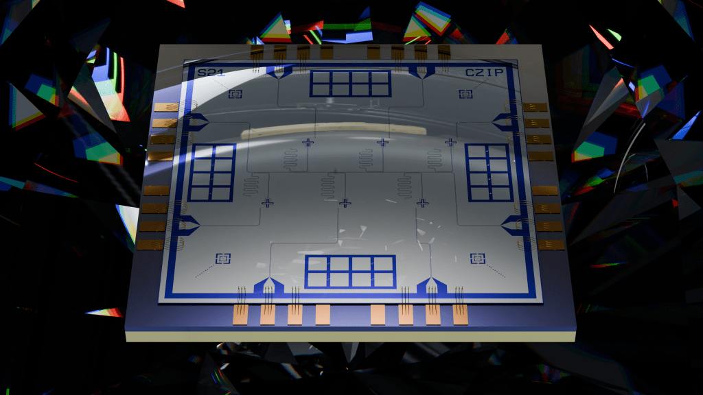
01—The Missing Motherboard for Quantum Computers May Be Superconducting
Quantum computers are usually introduced with one number: how many qubits they have.
That number matters. But every new qubit also creates a much less glamorous engineering problem.
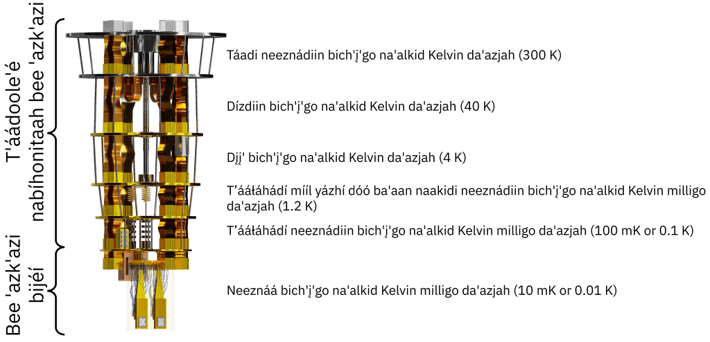
It needs control signals. It needs readout. It needs cables running between room-temperature electronics and a processor sitting deep inside a cryostat. Those cables have to pass through several temperature stages without adding more heat, congestion or hardware than the refrigerator can comfortably support.
So scaling a quantum computer is not only a question of building more qubits.
The classical control system has to scale with them.
A newly launched Finnish company called S-Transistors is building around that second problem. The VTT spinout announced on August 31, 2026 that it has raised €2.6 million to develop integrated circuits based on superconducting transistors, with a first product planned as a cryogenic multiplexer and a longer-term goal the company calls a “quantum motherboard.”
The funding is the news.
The control architecture is the interesting part.
02—More Qubits Create a Classical Electronics Problem
A superconducting quantum processor operates at temperatures measured in millikelvin.
Much of the equipment that tells it what to do does not.
Today, signal generation, control and part of the readout stack can sit at room temperature, connected to the quantum processor through coaxial cables and other wiring that descend through the dilution refrigerator.
This works. It is also one reason engineers keep studying ways to move more classical electronics into the cold environment.
The scaling relationship is easy to see.
If every additional group of qubits requires additional dedicated control and readout connections, the processor does not grow alone. The wiring, connectors, filters, amplifiers, control hardware and thermal load grow around it.
This is not just S-Transistors’ framing.
A 2026 Nature Electronics paper on superconducting digital control described individual signal lines as a major scaling challenge and demonstrated digital demultiplexing at millikelvin temperatures to distribute control pulses across multiple qubits.
The qubit count and the control stack are two sides of the same machine.
03—The Cryostat Has a Thermal Budget
Moving electronics closer to the quantum processor sounds straightforward until temperature enters the design.
At the coldest stages of a dilution refrigerator, cooling power is extremely limited.
That means an electronic circuit sitting near the qubits has to do useful work without turning its electrical power into more heat than the refrigerator can remove.
This is why cryogenic control research is not simply about shrinking room-temperature electronics and putting them inside the cryostat.
Power dissipation, thermal noise, cross-coupling and signal integrity all matter.
Researchers have already demonstrated several routes, including cryogenic CMOS and superconducting digital logic. A 2023 Nature Electronics study, for example, demonstrated a low-power cryo-CMOS multiplexer below 15 millikelvin while maintaining high single-qubit gate fidelity with appropriate filtering.
S-Transistors is entering the same broader problem from a different device layer.
Instead of beginning with conventional transistor logic adapted to cryogenic operation, it is trying to build control circuits around a transistor whose switching behavior is tied directly to superconductivity.
04—What S-Transistors Is Actually Building
The company’s core device is a superconducting transistor.
More specifically, the underlying VTT research describes a Josephson field-effect transistor, or JoFET.
A JoFET combines a gate-controlled transistor-like structure with a superconducting weak link. Instead of using the gate only to control an ordinary semiconductor channel, the gate can tune the superconducting current flowing through the device.
That gives engineers something unusually useful for cryogenic electronics: electrical control in a device designed to operate in the same low-temperature world as superconducting circuits.
The S-Transistors announcement describes the goal as combining transistor functionality with the ultra-low power dissipation associated with superconductivity.
That is an important distinction.
The company is not claiming that every circuit consumes literally zero power. The engineering target is to make control and signal-routing electronics far more compatible with the thermal constraints of a cryogenic quantum system.
The transistor is the building block.
The real question is what can be built around enough of them.
05—The Device Starts With Graphene and a Josephson Junction
The technical foundation is more concrete than the startup announcement alone suggests.
A 2024 Applied Physics Letters paper from VTT and Aalto University reported wafer-scale, CMOS-compatible graphene Josephson field-effect transistors.
The devices used monolayer graphene as the channel, an aluminum-oxide gate dielectric, and superconducting titanium/aluminum contacts.
The researchers demonstrated gate-tunable superconducting critical current across devices with gate lengths between 150 and 350 nanometers. For one 50-micrometer-wide device, the paper reports critical current reaching roughly 3 microamps.
The exact values are less important than what they establish.
The transistor can be controlled electrically.
The superconducting behavior is measurable and repeatable.
And the fabrication process was designed around wafer-scale methods rather than a single hand-built laboratory device.
That is the bridge between a physics experiment and something that might eventually become an integrated circuit platform.
06—Wafer-Scale Is the Part That Changes the Conversation
A superconducting transistor is interesting as a device.
A reproducible wafer process is what makes circuits possible.
VTT’s current announcement says the technology is already available at wafer scale. Earlier research provides useful detail behind that statement.
A 2025 VTT/Aalto conference paper on graphene JoFET fabrication reported a 98% device yield on a 150 mm wafer platform. The researchers also developed behavioral and physics models intended to support circuit design.
That does not mean a complete quantum motherboard is rolling off a production line today.
It means the work has moved beyond proving that one transistor can switch.
Integrated electronics require repeatability across many devices, predictable models for circuit designers, process control and eventually a manufacturing path that can produce useful circuits at acceptable yield.
S-Transistors is now trying to take that next step.
The company says part of its new funding will go toward establishing a manufacturing pilot line for superconducting-transistor integrated circuits.
07—The First Product Is a Multiplexer, Not a Motherboard
The words “quantum motherboard” make the long-term vision easy to imagine.
The first product is much narrower.
S-Transistors says it plans to build a superconducting-transistor-based multiplexer that plugs into existing cryogenic setups.
That sequencing makes engineering sense.
A multiplexer takes multiple signal paths and allows them to share a smaller number of physical connections or routing resources. Inside a cryogenic system, that can reduce some of the wiring burden without asking a quantum-computer developer to redesign the entire control architecture at once.
The company says the first multiplexer is intended for quantum-device development and prototyping and is planned to reach early customers and strategic partners within its first year of operation.
That creates a clean progression:
one transistor,
then a useful routing circuit,
then denser integrated control electronics,
and eventually the larger motherboard concept.
The motherboard is the destination.
The multiplexer is the first test of whether the device platform can become a product.
08—Why Multiplexing Matters So Much at Millikelvin Temperatures
Multiplexing is not a new idea in quantum hardware.
It keeps appearing because it attacks one of the most physical parts of the scaling problem: the number of wires entering a cryostat.
A 2025 Nature Communications paper on superconducting time-division multiplexing describes each signal line as a contributor to cryostat cost, occupied space and temperature stability.
A separate 2026 Nature Electronics demonstration integrated superconducting digital control electronics with qubits at millikelvin temperature and used digital demultiplexing to distribute control pulses across several qubits.
The approaches are different, but the design goal is related.
Instead of allowing the number of room-temperature connections to rise directly with every new controlled element, place smarter routing closer to the quantum device.
S-Transistors wants its first product to occupy exactly that layer.
If the multiplexer works as intended in existing cryogenic setups, the company gets to test the transistor technology in the place where its claimed advantage matters most: inside a real cold signal path.
09—A Quantum Motherboard Is Not a PC Motherboard
The analogy is useful, but it needs limits.
A PC motherboard connects a processor, memory, storage, expansion devices, power delivery and external interfaces on a shared physical platform.
S-Transistors is not proposing that same architecture at millikelvin temperature.
Its “quantum motherboard” refers to an integrated cryogenic control layer that sits much closer to the quantum processing unit and handles more of the signal orchestration locally.
Think of it as the missing classical layer around the QPU.
The quantum chip still performs quantum operations.
Room-temperature computers still participate in the wider system.
But some of the work that currently requires large numbers of individual connections between those worlds could move into cryogenic integrated circuits.
That is why the motherboard idea matters.
It shifts the scaling question from:
How many qubits can we fabricate?
to:
How many qubits can the complete machine control, read and connect without the surrounding infrastructure becoming the limiting factor?
10—The Control Layer May Need to Move Closer to the QPU
The closer control electronics move to the quantum processor, the less distance some signals need to travel before they are routed, selected or processed.
That can reduce wiring pressure.
It also changes the engineering tradeoffs.
Electronics closer to the qubits must coexist with a far more delicate thermal and electromagnetic environment than ordinary control hardware.
Cryogenic CMOS research has shown that transistor-based electronics can operate at very low temperatures. Superconducting digital logic has shown another route. Recent work has even demonstrated integrated quantum processors controlled by superconducting digital electronics at millikelvin temperature.
S-Transistors does not need those approaches to be wrong for its own approach to matter.
They establish something broader: quantum scaling increasingly includes co-design between the QPU and its classical control electronics.
The company is betting that a gate-controlled superconducting transistor can become a useful building block inside that co-design.
That is a more precise claim than saying one device will solve quantum scaling by itself.
11—The Motherboard Has to Be an Integrated Circuit Problem
One transistor can route one thing.
A motherboard requires systems of devices.
That is why S-Transistors’ move from wafer-scale JoFETs toward integrated circuits is the critical transition.
Circuit designers need device models.
Fabrication needs repeatability.
Logic and routing need predictable switching.
The architecture needs interfaces to the quantum hardware it is supposed to control.
Packaging has to survive repeated cryogenic cycles.
And the complete circuit has to fit inside a thermal budget that gets tighter as it moves closer to the coldest stage.
The earlier VTT research already addresses part of that foundation by reporting wafer-scale fabrication and developing models for JoFET-based circuits.
The new company is taking on the next layer: product prototypes, a dedicated cryogenic laboratory and a pilot manufacturing line.
That is why the €2.6 million round matters without becoming the center of the story.
It funds the transition from device physics into circuit engineering.
12—There Is More Than One Route to Cryogenic Control
Quantum hardware is not waiting for a single control technology.
Cryo-CMOS, superconducting single-flux-quantum circuits, adiabatic superconducting logic and other cryogenic electronics are all active areas of research.
That context is useful because it keeps the S-Transistors story in proportion.
A 2024 npj Quantum Information paper on adiabatic superconductor logic described the very small cooling power available near 10 millikelvin as a central constraint for conventional logic families close to qubits.
A 2026 Nature Electronics system showed that superconducting digital electronics can already control multiple qubits at millikelvin temperature with digital demultiplexing.
S-Transistors adds another device architecture to that landscape.
Its differentiator is the attempt to retain familiar field-effect transistor control while using a superconducting channel structure designed for extremely low-temperature operation.
The winner does not need to be one universal technology.
Future quantum computers may partition different control tasks across different temperature stages and different electronic technologies.
13—What Has Been Demonstrated, and What Is Still Planned
This is where the timeline needs to stay clear.
Already demonstrated in the underlying research:
wafer-scale graphene JoFET fabrication,
CMOS-compatible processing,
gate-tunable superconducting critical current,
and later work reporting high device yield on a 150 mm wafer platform.
Announced by S-Transistors:
a €2.6 million pre-seed round,
development of cryogenic signal-control prototypes,
a dedicated cryogenic laboratory,
a manufacturing pilot line,
and a superconducting-transistor multiplexer planned as the first product.
Still a longer-term goal:
the complete quantum motherboard.
That separation matters because a transistor platform and a finished control architecture are not the same thing.
The technical foundation exists.
The company now has to turn that foundation into circuits that quantum-hardware teams can integrate, characterize and use.
That is the stage the story is at today.
14—Why the 150 mm Wafer Matters More Than the Funding Number
Deep-tech announcements often lead with the size of the investment.
For this story, the more interesting number may be 150 millimeters.
That is the wafer size used in the 2025 fabrication work that reported 98% yield for the graphene JoFET platform.
A wafer result says something different from a funding round.
It says the researchers are thinking about process repeatability across many devices at once.
It also exposes the next questions naturally.
Can those devices be connected into larger circuits with consistent behavior?
Can useful multiplexers be fabricated with the same repeatability?
How does performance change when the circuit is packaged and connected to real quantum hardware?
What power, noise and switching characteristics appear at system level?
S-Transistors has not answered all of those questions publicly yet.
Its product roadmap is designed to start answering them.
That is a healthy way to read the announcement: not as the completion of a quantum motherboard, but as the beginning of the circuit-validation phase.
15—The Next Scaling Metric May Be Connections per Qubit
Qubit counts are easy to put on a chart.
Control architecture is harder to compress into one number.
But as systems grow, the ratio between quantum devices and the classical hardware needed to operate them may become just as important.
How many external lines are required?
How much control can be multiplexed?
How much power is dissipated at each temperature stage?
How much signal processing or routing can move closer to the QPU?
How much hardware sits outside the cryostat for every useful operation inside it?
Those questions do not replace qubit quality, gate fidelity or error correction.
They sit beside them.
A scalable quantum computer has to scale as a whole machine.
That is the deeper reason a superconducting multiplexer is worth watching even though it sounds much less dramatic than a new quantum processor.
Sometimes the limiting component is not the thing doing the computation.
It is the infrastructure that lets the computation happen.
16—The Real Upgrade Is Moving From More Qubits to a Scalable Machine
S-Transistors has attached a memorable name to its long-term goal: the quantum motherboard.
The name works because it points at a layer that is easy to ignore.
A quantum processor cannot scale independently from the classical system that controls it.
More qubits eventually mean more routing, more readout, more interfaces and more decisions about where electronics should live inside the temperature stack.
Superconducting transistors offer one possible way to move part of that work into the cryogenic environment without asking conventional room-temperature electronics to follow every signal all the way down.
The technology is not at the motherboard stage yet.
The first product is a multiplexer.
Before that sits a wafer-scale JoFET process.
Before that sits the physics of a gate-controlled superconducting current.
That chain is what makes the story interesting.
The next major upgrade in quantum computing may not arrive as another qubit.
It may arrive as the hardware that finally lets thousands of them behave like one scalable machine.